Home - Techniek - Electronica - Radiotechniek - Radio amateur bladen - Ham radio - Designing a microwave amplifier
Step-by-step procedure starts with specs, ends with results
Most people who aren't familiar with microwave technology regard microwave engineering as somewhat mysterious. Nothing could be further from the truth.
Often this opinion stems simply from limited knowledge of the subject, from a misconception that all power transmission requires a waveguide or "plumbing," or from a general lack of interest. Knowing that in microwave design, circuit performance is exceptionally dependent on layout(1) and understanding the mathematics associated with field theory and the use of distributed parameters for impedance matching, it's possible to conclude that microwave engineering is an arcane art limited to the very few. Not so!
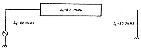
Fig. 1 - Mismatch occurs when 25-ohm load is inserted directly in 50-ohm system.
S-parameters
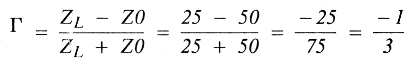
Manufacturers of microwave electronic components, namely transistors, characterize these devices according to scattering parameters known also as "S" parameters. S parameters are simply voltage reflection coefficients that possess both magnitude and phase. Consider a 25-ohm resistor at the end of a 50-ohm transmission line (fig. 1). The reflection coefficient of the 25-ohm load is computed as follows:
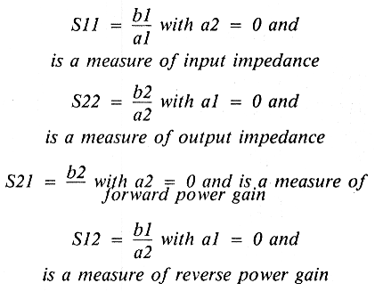
Γ can be complex and is simply a reflection coefficient; that's what an S parameter is - nothing more than a reflection coefficient. The S parameters are measured values and give an indication as to the performance of the device, and are generally measured in a 50-ohm system. It's more practical to construct a 50-ohm termination than to rely upon open circuits and short circuits and attempt to characterize a device with "Y" or "Z" parameters. The four S parameters specified are S11, S12, S21, and S22 (see fig. 2).
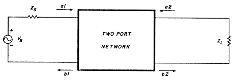
Fig. 2 - Two-port network used to define S parameters.
S parameters are simply related to power gain and mismatch loss, quantities which are often of more interest than the corresponding voltage functions.
It's important to understand that S parameters are measured parameters and give the designer a real-world indication as to how the particular transistor will work. Generally, a designer's most important considerations are power gain, noise figure, stability, biasing, and a necessary matching structure for reasonable VSWR.
A transistor is a bilateral device, with the amount of bilateral interaction defined by S12. Analyzing the performance of an amplifier operating as a bilateral device is a tedious process, and one has to resort to the use of computers and commercially available programs such as Super-Compact, a rather powerful microwave circuit design optimization program. For the purpose of illustration, we will assume a unilateral device (S12 = 0.0).
Using the data sheet
Suppose someone gives you several NEC NE388 GaAsFET transistors and a data sheet, then asks you to design an amplifier that's to operate at 3 GHz. Approximately how much gain should you expect to achieve? What would the input and output matching network look like?
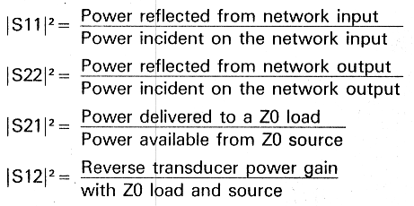
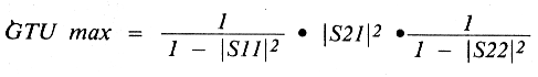
Start by reviewing the data sheet for the FETs. (For this design, noise figure is not a consideration.) The load impedance and source impedance are both 50 ohms. The device is a GaAsFET. You'll also notice that the S parameters are specified at Vps = 3.0 volts and ID = 10 mA. Therefore, for the matching network to be effective and for the gain calibration to be meaningful, the device must be biased at these values of Vps and ID. Try to get a feeling for maximum usable gain, i.e. the Gain Transducer Unilateral (GTU). (This assumes a unilateral device where S12 = 0 and a matched source and load condition exists.) This was derived from the more general equation for GT (Gain Transducer) under the conditions specified above.
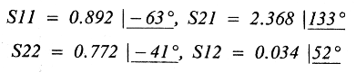
At 3000 MHz,
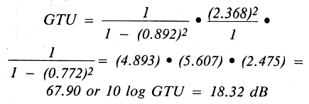
This computation is consistent with the data sheet. Notice that in addition to providing a table of S parameters for the packaged devices, S parameters are given for NE388 chips as well, and the S parameter data is listed for frequencies from 2 to 10 GHz in 0.5-GHz step increments. Note that S11 and S12 are both capacitive, but become more inductive as frequency increases.
S11 represents approximately 10 - j80 ohms and S22 represents approximately 50 - j120 ohms. For optimum performance and power gain, the transistor's input and output impedances should be matched to 50 ohms.
One suitable way of constructing this amplifier is a technique called microstrip. Microstrip possesses transmission line characteristics and is essentially just conductive runs over a conducting ground plane, with an intermediate substrate in between.
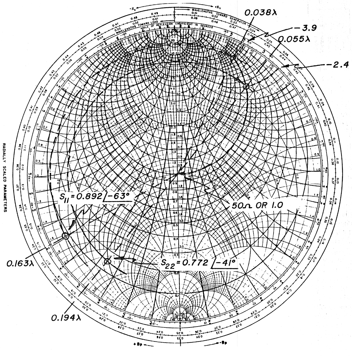
Fig. 3 - GaAsFET, NE388 matching using Smith Chart.
Matching procedure
The idea is to "move" S22 and S11 to the 50-ohm center of the Smith Chart (fig. 3). In both cases, this is done by rotating on a length of transmission to the constant conductance circle that is coincident with the center of the Smith Chart or the 50-ohm location and then adding a parallel capacitor of the appropriate size. For the S22 match, a length of line 0.194X + 0.055X = 0.249X is used to rotate to constant conductance circle coincident with 50 ohms; for S11 the length of line is:
0.163λ + 0.038λ = 0.201λ.
Y(S22) = 2.4 = Y/ B0
Since our transmission line characteristic is Z0 and is 50 ohms,
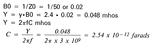
A 2.54 × 10⁻¹²F (2.54 pF) capacitor shunting the transmission line to ground will add enough susceptance to complete the output match to 50 ohms.
A similar procedure is used to match the input to 50 ohms.
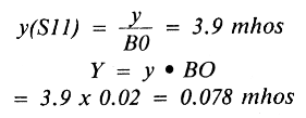
A 4.138 × 10⁻¹²F (4.138 pF) capacitor shunting the transmission line to ground will add enough susceptance to complete the input match to 50 ohms. Thus far, what we have represented is shown schematically in fig. 4.
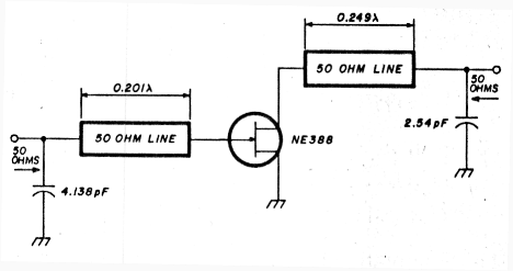
Fig. 4. Component values determined for GaAsFET input/output match.
Microstrip components used
The microstrip substrate is a teflon material with a dielectric constant of 10.0. The distributed characteristics of microstrip will be utilized to synthesize the 50-ohm transmission line and shunt capacitors. The lengths of the input and output transmission lines are 0.201λ, and 0.249λ, respectively.
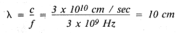
The equation relating frequency and wavelength is c=fλ, where c is the velocity of light and is 3 × 1010 cm/sec. In air, the wavelength of a 3-GHz signal is
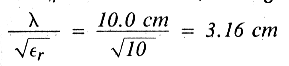
or approximately 3.937 inches. The effective wavelength in a material other than free space is the wavelength in free space divided by the square root of the dielectric constant. For a substrate whose dielectric constant is 10.0, the effective wavelength is
or 1.2449 inches. The length of the input matching section is 0.201X and the length of the output matching section is 0.249λ. This in air would represent (0.201λ) (3.937 inches/λ) = 0.7913 inches and (0.249λ) (3.937 inches/λ) = 0.9803 inches.
In a substrate with a dielectric constant of 10.0, the real lengths of the input and output become (0.7913 inches) (0.3162) = 0.2502 inches and (0.9803 inches) (0.3162) = 0.3099 inches, respectively.
The characteristic impedance of microstrip, Z0 is:
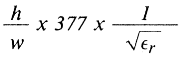
The impedance selected for our line is 50 ohms and ε2 = 10.0. The substrate thickness is 0.020 inches. Solving for ω:
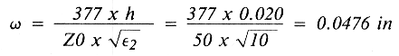
Thus the width of a conductor whose characteristic impedance is 50 ohms on a substrate whose thickness is 0.020 inches, with a dielectric constant of 10.0, is 0.0476 inches. The original schematic takes on a new aspect - dimensions (see fig. 5).
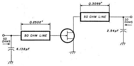
Fig. 5. Transmission line physical parameters determined from requirements.
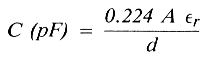
The input capacitance of 4.138 pF and output capacitance of 2.54 pF will be synthesized using microstrip techniques. Generally, if the width of a segment is twice as wide as the length, the section looks like a shunt capacitor.
The capacitance of a parallel plate capacitor is:
where:
A is the area of the plate in square inches
d is the separation of the plates in inches
εr is the dielectric constant
Solving for A:
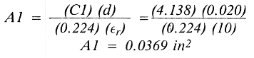
Similarly:
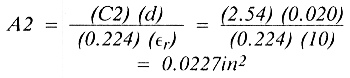
We wish to make the width of the section twice as wide as the length. Therefore,
Similarly:
The circuit now takes on the appearance of that shown in fig. 6.
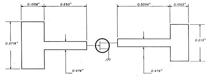
Fig. 6. Input and output matching structure dimensions.
The basic radio frequency input and output matching structure is now defined.
This matching structure was based on S parameters which were stated for a given Vps and IDs. A GaAsFET device is a transconductance device; this simply means that it's a voltage-controlled current source.
Feedback and biasing
This brings up the means by which the devices should be biased. A quick glance at the data sheet reveals the NE388 will require a VGS of approximately -3.0 volts to maintain a VDS = 3.0 volts and IDs = 10.0 milliamperes. But the VGS necessary to maintain these aforementioned bias conditions can vary between -2.5 to -3.5 volts - a production nightmare, especially if the unit must operate between -55 and +70°C. Solution: use a servo - i.e., a feedback circuit!
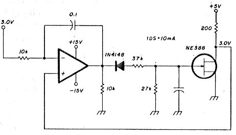
Fig. 7. Feedback network improves amplifiers temperature-handling capability.
I suggest the circuit shown in fig. 7 because I know it work well over a wide range of temperatures. The microwave matching network components are left out for simplicity.
The three critical items in this circuit are the stability of the + 5.0 volts, the accuracy and stability of the 200-ohm resistor, and the 3.0-volt reference. The diode prevents the possibility of a positive voltage being applied to the gate. A positive voltage on the gate without considerable current limiting would damage the device.
The voltage divider consisting of the 37.4-k and 27.4-k resistors prevent the gate to source voltage from exceeding - 8.0 volts during initial turn-on. The dc bias, namely the Vps and Vag is applied to the NE388 through the use of high-impedance, quarter-wave, short-circuited stubs. The short circuit at 3 GHz is accomplished by wire-bonding the end of the stub to a 100-pF chip capacitor that is connected to ground. Remember, a quarter-wave long transmission line short-circuited on one end looks like an open circuit on the other. The design procedure results in the realizable 3-GHz amplifier circuit shown in fig. 8.
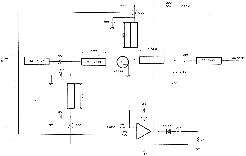
Fig. 8. Complete distributed and lumped component 3GHz amplifier circuit.
Notes
- You don't wire a 4-GHz amplifier the same way you'd wire a car. Consider that a piece of No. 26 wire measuring 0.050 inches long represents an impedance of j25 ohms at 4.0 GHz. This would introduce a voltage SWR (mismatch) of 1.63:1, with 5.8 percent of the power reflected back to the generator should this wire be connected in series in a 50-ohm system.