Home - Techniek - Electronica - Radiotechniek - Radio amateur bladen - Ham radio - A two-loop 10-Hz step 40 - 70 MHz Synthesizer
Achieve good image rejection without sacrificing resolution, tuning speed, locktime, and stability.
Using a 40-70 MHz local oscillator is generally accepted as a means of achieving good image rejection in modern HF design. The frequency stability and accuracy of such an oscillator is achieved through synthesis. Often contradictory design requirements are high resolution, tuning speed, low noise output, spectral purity, low power consumption, small volume, and low price.(1-4) Most of the designs use many loops to obtain small step resolution. This article shows a method to overcome this difficulty.
The algorithm
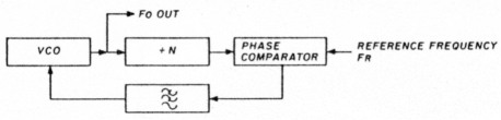
Fig 1 - Loop diagram for simple one-loop synthesizer.
Normally, unless special techniques are employed, the step size is equal to the reference source frequency. Figure 1 shows a block diagram of such a loop. You must use a low reference frequency to provide high resolution. However, with step sizes less than 1 kHz, locking time and close-in noise are degraded. For instance, to achieve 10-Hz resolution in the 40-70 MHz range, it is usually necessary to use four or five loops.
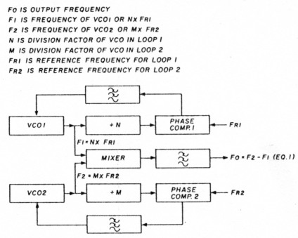
Fig 2 - Algorithm for present synthesizer.
Figure 2 illustrates a two-loop block diagram that meets the combined requirements. To achieve short locking times and low noise output it is necessary to use substantially highleferencefrequencies - e.g., 10 kHz. If we put Fri = 9.99 kHz and Fr2 = 10 kHz in fig. 2, we can rewrite eqn. 1, Fo = F2 - F1, from fig. 2 as:
where N and M are as defined in eqn. 1
To make 10, 100, or 1,000-kHz steps (or their multiples), change only the divider, M. For steps of 10,100, or 1,000 Hz (or their multiples), you have to change the values of N amd M to maintain M - N unchanged.
For instance, if you need a step 30 Hz up, increase N by 3 (3 × 0.01 = 30 Hz) and M by 3. So,
Finitial = [10 × (M - N) + 0.01 × N] kHz
Ffinal = [10 × (M + 3 - (N + 3)) + 0.01 × (N + 3)] kHz
Step = Finitial - Ffinal = 0.03 kHz = 30 Hz
Derivation of design equations
One of the problems of 40-70 MHz synthesis using one loop is the rather high relative range: 30 MHz in a 40-M Hz VCO. One of the advantages of the present method is that you can use two VCOs in a higher VHF band, making the relative range a minor problem. (In our units we have used F1 at 160-200 MHz and F2 at 120-130 MHz, both single loops.)
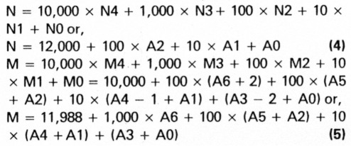
Now let's derive the design equations for these arrangements. Remembering that the output frequency is a seven-digit decimal number (e.g., 47,936.42 kHz), put:
Fo = 10,000 × A6 + 1,000 × A5 + 100 × A4 + 10 × A3 + A2 + 0.1 × A1 + 0.01 × A0 (in kHz).
Similarly the division factors N and M may be written, as they are integers:
(F1 and F2 < 1,000 MHz, so Mi = Ni = 0 for i > 4).
N = N0 + 10 × N1 + 100 × N2 + 1,000 × N3 + 10,000 × N4
M = M0 + 10 × M1 + 100 × M2 + 1,000 × M3 + 10,000 × M4
Using eqn. 2 you have:
10,000 × A6 + 1,000 × A5 + 100 × A4 + 10 × A3 + A2 + 0.1 × A1 + 0.01 × A0 = 10 × (M0 - N0 + 10 × (M1 - N1) + 100 × (M2 - N2) + 1,000 × (M3 - N3) + 10,000 × (M4 - N4)] + 0.01 × (N0 + 10 × N1 + 100 × N2 + 1,000 × N3 + 10,000 × N4)
Equating the corresponding terms you have:
Because the Ai are given numbers, you have eight equations with ten unknowns to determine Ni and Mi. This gives you two degrees of freedom to locate the ranges of F1 and F2. (You must establish values for two parameters, so choose N4 at first.) If the values you choose for N4 (and M4) are too high, the dividers (which can be preset) may fail to operate and the noise perfor mance will be poor because of the great division factor. But if N4 is too small, you'll have problems with the relative range of the VCO. In the present case, a good choice will be 1 for N4 (and M4).
The range of F1 (N loop) is ≈ 10 MHz because, to cover 9.99 kHz (the maximum step not covered by the M loop alone) in steps of 10 Hz, we have 1,000 channels with 9.99 kHz of reference frequency, which gives 10 MHz. So, the F2 (M loop) range is 10 MHz + 30 MHz (range of the output) = 40 MHz.
The other degree of freedom permits you to fix the value of N3. Choose 2 for this (meaning that with N4 = 1, for ≈ 10-MHz range, we have F1 ranging from ≈ 120 to 130 MHz, and, consequently, F2 ranges from = (120 + 40) = 160 to ≈ (130 + 70) = 200 MHz. These frequencies are convenient enough for the dividers and relative ranges of the VCOs.
Now rewrite the expressions of N and M using eqn. 3 and the chosen values for N3, N4, and M4:
As the output ranges from 40,000.00 to 69,999.99 kHz, the value of A6 maybe 4, 5, or 6. A5, A4, A3, A2, A1, and A0 may be 0 to 9. Now it's possible to calculate the exact ranges of N, M, F1, and F2:
a. Minimum N: A2 = Al = A0 = 0.
From eqn. 4: Nmin = 12,000.
b. Minimum Fi: (fig. 2) F1min = 9.99 × Nmin = 119,880 kHz.
c. Maximum N: A2 = Al = A0 = 9.
From eqn. 4: Nmax = 12,999.
d. Maximum F1: (fig. 2) F1max = 9.99 × Nmax = 129,860.01 kHz.
e. Minimum M: A6 = 4; A5 = A4 = A3 = A2 = Al = A0 = 0.
From eqn. 5: Mmin = 15,988.
f. Minimum F2: (fig. 2) F2min = 10 × Mmin = 159,880 kHz.
g. Maximum M: A6 = 6; A5 = A4 = A3 = A2 + A1 = A0 = 9.
From eqn. 5: Mmax = 19,986.
h. Maximum F2: F2max = 10 × Mmax = 199,860 kHz. For example, suppose that you want to synthesize an output of 56,721.98 kHz. Then A6 = 5, A5 = 6, A4 = 7, A3 = 2, A2 = 1, A1 = 9 and A0 = 8.
Using eqns. 4 and 5 you have:
N = 12,000 + (100 × 1) + (10 × 9) + 8 or, N = 12,198 and
M = 11,988 + (1,000 × 5) + (100 × (6 + 1)) + (10 × (7 + 9)) + (2 + 8) or,
M = 17,858
So, F1 = 9.99 × 12,198 = 121,858.02 kHz and F2 = 10 x 17,858 = 178,580 kHz.
It works because Fo = F2 - F1 = 56,721.98 kHz.
The algorithm shows that this is a type of synthesis which is convenient to implement with microprocessor control. The calculations become even more involved when two-modulus prescalers are used within the loops.
The complete design
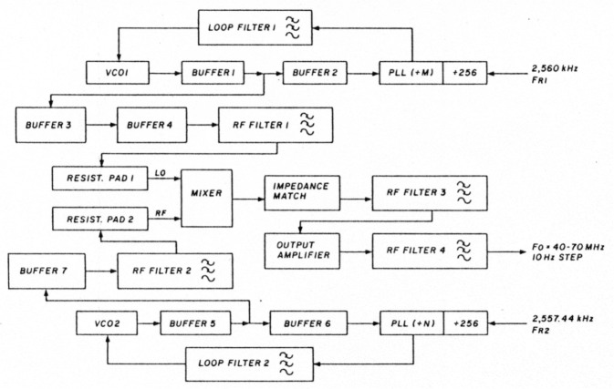
Fig 3 - Block diagram for the present synthesizer.
Our particular assembled unit has been built according to the block diagram in fig. 3. The PLL blocks each include one two-modulus prescaler. We used MC-12016(5), 40/41 type); we have built them with MC-145156(6) PLLs. However, if you use the MC-145158, the reference frequency problem may be easier to solve by entering only one reference in both loops (e.g. 9,990 MHz - and programming the reference dividers with 999 for the M loop and 1,000 for the N loop). We've used the PD phase detector output (from the phase comparator of the PLL) to avoid operational amplifiers in the control lines. The resulting reference rejection has been better than 60 dB down.
Now let's analyze each block of fig. 3:
a. VCO 1 and 2: Because their frequencies fall in the VHF range, the low noise J-FET, like the U-310 (or the plastic J-310 family), is a convenient transistor choice.(7),(9) If you don't plan to pretune, take care in your layout and choice of components to permit VCO 1 to cover its 40-MHz range.
b. Buffers 1, 2, 3, 6, and 7 may employ bipolar transistors like the BFY-90 for low noise, high isolation, and broadband operation. Buffer 5 may be a dual-gate MOSFET - try the MFE-521 or 3N-211(7). For buffer 4 use a high output level broadband linear transistor (a BFW16A) to get a suitable signal power for the mixer LO input.
c. We chose an SRA-1 bridge diode double-balanced mixer from Mini Circuits to get a very low spurious response. This is very dificult to obtain using other types of mixing devices. For this purpose we've had to "clean" both LO and RF port signals concerning harmonic content with RF filters 1 and 2. Two resistor pads have been used to couple both signals to the mixer under correct resistive impedance (50 Ω).
d. A BFY-90 stage presents the correct resistive load to the mixer (50 Ω. Its output passes a third RF filter to block the harmonic power (now generated by the mixer itself) and drives the final IBFW-16A) amplifier stage through another BFY-90 stage. This gives a high-level power (= 12 dBm) to the first mixer of the receiver. RF filter number 4 maintains the output free from harmonics.
Final comments
This article presents an algorithm rather than a circuit design. The synthesizer itself may be built using all the standard techniques for low noise operation, like in-loop mixing for lowering the division factors, low noise phase comparators (HEF-4750(8) series from MULLARD), and pretuned systems to get quieter varactor control. All these techniques are fully described in the literature(2),(3) so we won't discuss them here. The only point we'd like to emphasize is that the higher the division factors, the poorer the close-in noise, because the noise from reference is multiplied by a greater number and we have a worse signal-to-noise ratio at the phase comparator. So, without in-loop mixing (or another equivalent technique to diminish N and M1, special care must be taken with crystals and crystal oscillators to minimize in-band noise.(9)
Concerning stability and accuracy, note that 10 Hz in 200 MHz means 0.05 ppm, so that the use of simple "non-mastered" reference sources doesn't seem to make sense.
Conclusions
We've presented a method to synthesize three million 10-Hz channels (40-70 MHz) with a reference-to-step ratio of 1,000 by using only two loops. We have used the frequency difference between the two loops, but the sum may be used in the same manner as long as you take care that the spurious and harmonic signals don't fall within the output band region.
References
- Ulrich L. Rohde, DJ2LR/KA2WEU, Digital PLL Frequency Synthesizers-Theory and Design, Prentice Hall.
- V. Manassevitch, Frequency Synthesizers-Theory and Design, John Wiley Et Sons.
- W.C. Lindsey and M. K. Simon, Phase-locked Loops and Their Application, IEEE Press.
- W.F. Egan, Frequency Synthesis by Phase Lock, John Wiley Et Sons.
- Motorola MECL Data Book, Series C, Motorola, Inc. 1982.
- Motorola CMOS/NMOS Special Functions Data, Series A, Motorola Inc., 1984, pages 6 95 to 6-119.
- Motorola RF Data Manual, Motorola Inc., 1980.
- Philips, Digital Integrated Circuits-LOCMOSNE4tXVBFamily, N.V. Philips Gloeilampenfabrieken, 1980.
- W. P. Robins, Phase Noise in Signal Sources I Theory and Application), IEEE Telecommunications Series 9.
PY1LL, Luiz C. M. Amaral and Carlos Alexandre C. Mathias.