Home - Techniek - Electronica - Radiotechniek - Radio amateur bladen - Practical Wireless - The PW Chatterbox 1
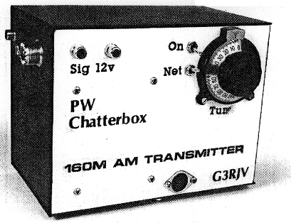
1.8MHz AM transmitter and receiver, part 1
There's been a lot of interest in 1.8MHz a.m. operation recently. To get you on Top Band', the Rev. George Dobbs G3RJV and Ian Keyser G3ROO, have come up with the PW Chatterbox, a complete a.m. station.
The amateur band between 1.8 and 2MHz is a little odd, in that we rarely hear anyone calling it 1.8MHz. More often it's referred to by its affectionate nickname `Top Band'.
If you talk to any radio amateur who has been licenced for 20 years or more, and mention `Top Band', you'll see his eyes glaze over! The corners of his mouth will then begin to rise, and you'll hear endless stories of the Sunday morning nets on a.m.
The local `natter' on Top Band, particularly using a.m. equipment, has a firm place in the folklore of amateur radio. It's something many of us have grown up with, and now you can join in too!
The Idea
In recent years I have had few excursions on the band, except for the occasional relaxing c.w. QSO. It's a pleasant band, a place to relax and make friends. Despite this, I must admit to being a little surprised, when PW's editor asked me if I had thought of designing an amplitude modulated transceiver for 1.8MHz.
Apparently, the idea originated as a request from readers. It seems that, almost unknown to me, groups of radio amateurs had been forming a.m. nets on the band. It sounded like fun, and so the `Chatterbox' project was soon under way.
The Chatterbox
The Chatterbox is designed as a rig for the local 1.8MHz a.m. net, although I will describe how it can be used on c.w. with up to 10W input. But you should bear in mind that the basic design is dedicated to a.m. use.
The Chatterbox is made up of a separate transmitter and receiver. This approach goes back to the old days of 1.8MHz equipment, but I must admit that nostalgia was not the primary aim.
I decided that when building an a.m. receiver for local use, it's very much easier to have separate units. I also think that many people will only want to build the transmitter, as they'll already have a suitable receiver.
Simple Receiver
The receiver portion of the Chatterbox is a simple a.m. only design, capable of matching the performance of the transmitter. If you require a 1.8MHz DX receiver, you'll have to look elsewhere!
To fall in line with these ideas, the prototype transmitter and receiver were built in separate, but linked, boxes. The styling is rather like the famous B2 `Spy' transmitter-receivers, once so popular on the bands.
When I began work on the project, I spoke to Ian Keyser G3ROO, and we were soon working jointly on the idea. There are few problems in getting a solid state, IOW c.w. signal on 1.8MHz. The problem comes when you're looking for the easy production of amplitude modulation.
Ian told me of the excellent a.m. signal put out on the band by Doug G4RGN, on a 1.8MHz net in Kent. Doug very kindly supplied us with his circuit, which is simple, neat and works very well and it forms the basis of the Chatterbox transmitter.
The transmitter is a real joy to use. The p.a. stage is almost `bomb-proof' and is very efficient. You can obtain 10W out for approximately 12W input. I could almost claim that it's a solid state switch working at a frequency of 2MHz!
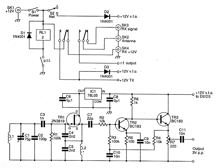
Fig. 1.1: The PW Chatterbox v.f.o. circuitry (below) with the switching and control circuitry shown above.
Familiar Circuit
The circuit of the v.fo. is shown in Fig. 1.1. It's that familiar favourite, the parallel tuned Colpitts circuit that I, and hundreds of others use whenever a v.f.o. is required for the h.f. bands.
The v.f.o. is capable of high output and has a preset, R7, to control the output. This may require adjustment for optimum results, and the best modulation quality.
Good quality polystyrene capacitors are used for the frequency determining portions of the circuit. The capacitors involved are C2-5.
The v.f.o. tuning inductor, L 1, is close-wound on a 7mm former with a core (Maplin LB17T or similar surplus former). I hold the turns in place with bees wax to add stability. Mechanical stability is important throughout the v.f.o. Although oscillator stability should present few problems at 2MHz, a badly built v.f.o. will drift.
Extra stability is provided by two stages of buffering amplification, coupled with a regulated supply line for the f.e.t. oscillator stage. The v.f.o. should be built in its own screened box. It also requires a slow motion drive and I used a 6:1 vernier drive and dial in the prototype.
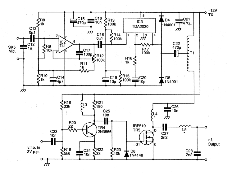
Fig. 1.2: The Chatterbox modulator (above), driver and power amplifier stage (below) circuitry.
Transmitter Board
The circuit for the main transmitter board is shown in Fig. 1.2. This board contains both the transmit stages and the amplitude modulator.
The modulator forms the top part of the circuit diagram and the transmit driver and power amplifier the lower portion. We'll consider the r.f. portion of this stage first.
The output from the v.f.o. is fed into a single driver stage, which is a 2N3866 bipolar transistor. A homewound r.f. choke, L3, damped by a 1805 resistor forms a wideband load.
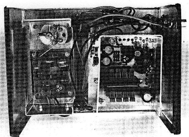
The completed Chatterbox transmitter section. The v.f.o. section is to the left, with the variable capacitor for frequency control visible in the top left hand corner of the picture. The power amplifier and modulator stages are to the right, with the modulation transformer shown located in the middle of the 'u' shaped combined heatsink and screening panel (see text).
Power Amplifier
The power amplifier is an IRF510 power f.e.t. with an r.f. load comprising L4. This stage is modulated with the aid of an audio frequency transformer, T1. The output has a low pass filter formed around L5 and C28.
The diode, D6, acts as a d.c. restorer. The f.e.t. requires a turn-on voltage of 3V. This voltage is obtained by rectifying the drive, so that if the drive fails, the p.a. stage turns off so it won't overheat.
The d.c. restoring action ensures that the drive waveform is positive-going, and the negative half is not wasted, and as the required drive for full output is at least 20V peak-to-peak, it avoids possible damage from excessive negative gate voltage.
The output low pass filter also looks rather odd. But it works! As the internal capacitances of the f.e.t. are large, it's necessary to use series capacitance on the input of the filter. The power amplifier stage is capable of delivering 8 to 10W of r.f. output.
The Modulator
The modulator is built around two i.c.s, a 741 preamplifer and a TDA2030 power amplifier. The overall gain is set at the preamplifier stage with a preset control.
The circuit closely follows the manufacturers data for the TDA2030. This is a very useful, beefy audio amplifier which works very well and reliably in this application.
The modulation transformer, T1, is a centre-tapped transformer in series with the power f.e.t. The transformer is a homewound job using a special former, the R.S. Components Ferroxcube 228-264. This is also available from Maplin Electronics as part FT33L.
The cores used are designed for power oscillators and switch mode power supply systems. The component is made up from the two `E' shaped halves of the ferrite core, and a moulded former.
Take great care when handling the ferrite sections, as they are very brittle. During the testing of the prototype transmitter, two cores were damaged in the post. Broken ferrite sections can be glued together, and still used, but it's better not to break them in the first place!
Transformer winding
The transformer is wound on the moulded former, and the E shaped ferrite cheeks are then added to the assembly. The transformer requires 300 turns of wire, centred tapped for the audio input.
The transformer can be made by winding on 150 turns, making a tapping and then adding a further 150 turns. I tried several methods and wire gauges and decided upon a bifilar winding of 150+150 turns of 0.4/0.5mm (26s.w.g.) enamelled copper wire.
The original prototype had 300 turns, centre tapped and wound with 0.71mm wire, but this can only be achieved with careful winding on a lathe. In practice however, the bifilar winding using the wire suggested above produced the same results withoutoverheating problems.
The easiest method of making the transformer is to buy two small reels of 0.4/0.5mm wire, and then use them both in the winding process. The windings are made side by side. To make the job easier, you can mount the reels on a thin rod to act as a spindle, allowing them to turn freely as the wire pays out.
The winding consists of turns made with the two wires side by side. You should treat the wires as one wire. Start the operation carefully, and as neatly as possible, wind on 150 turns.
Distribute the winding as evenly as possible over the whole width of the former. Don't forget to leave about 150mm of wire free at both ends of the turning. The completed job will result in four ends of wire, two starts and two ends. If you've got more than this - something's wrong!
The necessary tapping is made by joining the end of one winding to the beginning of the other. The correct wire for the connection may be sorted out using a testmeter. These connections MUST be correct. If they aren't, the transformer won't work. If there's any doubt, carefully check. Don't forget that the order of the windings to complete the transformer is: beginningto-end to beginning-to-end.
Chatterbox Switching
Shown in the top half of Fig. 1.1, are the switching arrangements for transmit and receiving on the Chatterbox. The press-to-talk switch on the microphone, controls a 12V two-pole change-over relay.
One pole of the relay moves the antenna input from receive to transmit. The other pole, places 12V on to the v.f.o. and transmitter boards when the p.t.t. switch is pressed.
Unusually, the v.f.o. is switched off during the receive periods. This is not usually advised in normal transmitter practice, because of switch-on drift. In this application however, with an a.m. transmitter on 2MHz, the effects of short term drift is relatively unimportant.
Should the transmitter be required for frequent use on c.w., it would be advisable not to switch the v.f.o. off on receive. It may be better to provide an offset to remove it from the receiver passband.
The switch, S2, is a net switch to locate the transmitter frequency prior to transmitting. It switches the v.f.o. on, which then provides enough r.f. to locate the transmitter frequency. For accurate netting it may be advisable to switch on the receiver b.f.o. The switch, S 1 is the main on-off switch.
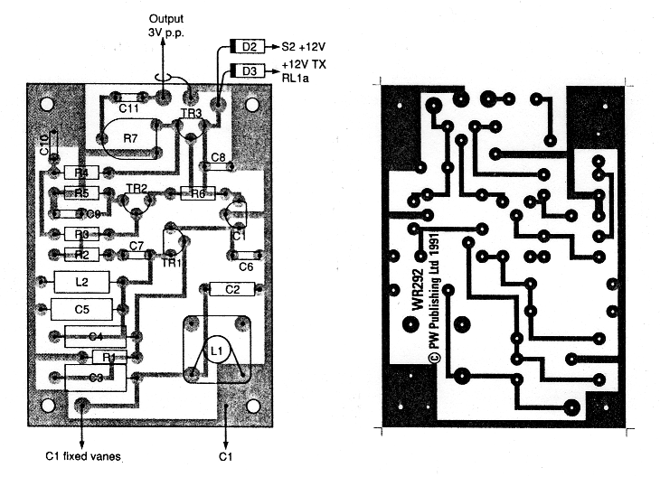
Fig. 1.3: Layout of the v.f.o. p.c.b. with component overlay (left) with the underside of the single-sided p.c.b. showing copper tracks, on the right.
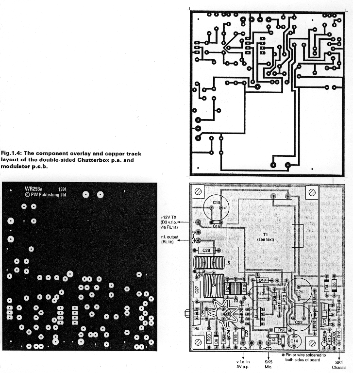
Fig. 1.4: The component overlay and copper track layout of the double-sided Chatterbox p.a. and modulator p.c.b.
Building The Boards
Layout of the v.f.o. board is shown in Fig. 1.3, and the layout of the main transmitter board is shown in Fig. 1.4. Following usual practice, the v.f.o. board is single-sided, although the transmitter board is double-sided to aid stability.
Just visible running around the edge of the p.c.b. is Fig. 1.4, is the simple wrap-round heatsink which is used for the p.a. f.e.t. and the audio amplifier chip. The heat-sink is homemade from aluminium and is 70mm high. The best method of making the heatsink, is to cut and file the metal to suit the individual p.c.b..
Heat Precautions
The f.e.t. used in the p.a. requires an insulated mounting kit to isolate the device from the heatsink. However, the TDA2030 audio amplifier i.e. doesn't require insulation from the heatsink in this single rail configuration.
At this stage, I recommend that TR5 and IC3 are attached to the heatsink before their leads are soldered to the board. This simple precaution will dissipate the heat involved during the soldering process.
Testing Time
I suggest that you should start by building and testing the v.f.o. first. It's easy to locate the oscillator on a suitable 1.8 MHz receiver, when its in the c.w. or s.s.b. mode.
The core of the tuned circuit should be adjusted for the required band coverage. With the values given, the v.f.o. will cover the whole of the 1.8 to 2MHz band, and you should check carefully to see that the v.f.o. doesn't stray 'out of bounds'. This is best done with an accurately calibrated receiver, frequency meter or crystal calibrator.
In practice, the ability of the v.f.o. to cover the entire allocation is useful for c.w. Don't forget that the whole band is not used for a.m. operation, and you wouldn't be popular if you used an a.m. signal on the bottom sector of 1.8MHz!
Setting Up
The transmitter is easy to set-up. It may be done by ear, or by using a cheap audio oscilloscope to monitor the signal.
If an oscilloscope is available, you should set it upon an high input audio range. The transmitter must be fed into a 50Ω dummy load capable of dissipating 10W.
There should be enough r.f. available, for you to lay the probe close to the dummy load, enabling the 'scope to display the classic trace of an a.m. signal.
The next stage is to adjust the r.f. level using the v.f.o. preset control, and the audio gain preset control on the transmitter board, to obtain the best modulation level consistent with good quality. If a 'scope is not available, connect the transmitter into the dummy load, and monitor the signal on an a.m. receiver. The presets are adjusted for the highest, good quality output.
Microphone Surprise
Surprisingly, I found that a cheap CB-type microphone produced the best quality. If you don't have a microphone handy, the Maplin Electronics Communications Microphone type WFO5F gave very acceptable results.
The transmitter is easy to use, and all you do is point and fire! The only other adjustment is to net onto the required frequency. Then you press the microphone switch and talk. I know there's at least six Chatterbox transmitters already in use, and they're all producing good quality signals on 1.8MHz.
The finished project ..read next month for the receiver part of the 'Chatterbox'
Errors And Updates
Wrong Toriodal Core. The PW Chatterbox transmitter parts list, page 23 of the August 1991 issue of PW, has L5 described as being wound on a T50-12 toroid. This is incorrect. The inductor L5 should be wound on a T50-2 toroid. Our apologies to those who've the started to build the transmitter.