Home - Techniek - Electronica - Radiotechniek - Radio amateur bladen - QEX - Understanding Switching Power Supplies, Part 1
Many find switching supplies mystifying.
Let's begin a tour through that strange land.
This is the first of a series of articles that will explain how switch-mode power supplies work in detail. They will give enough information to design several different types of switching power supplies.
There are two broad classes of power supplies: linear and switching. Linear supplies use time-continuous control of the output. Switching supplies are timesampled systems that use rectangular samples to control the output. There are three types of switching power supplies. Charge pumps manipulate the charge on a capacitor to change voltage. They can be used to increase voltage or invert the voltage. Buck and boost switching supplies use an inductor to provide the voltage conversion and regulation to either increase the voltage (a boost regulator), to reduce the voltage (a buck regulator) or invert the voltage (voltage inversion boost regulator). These articles focus on the buck and boost types of supply.
Inductor Basics
The important features of an inductor are that the current through it cannot change instantaneously and the voltage across the inductor is a result of the change in inductor current. This means that the voltage across the inductor will be positive (with respect to the polarity dot) when you charge the inductor and negative when the inductor is discharging. This allows the voltage to change essentially instantaneously.
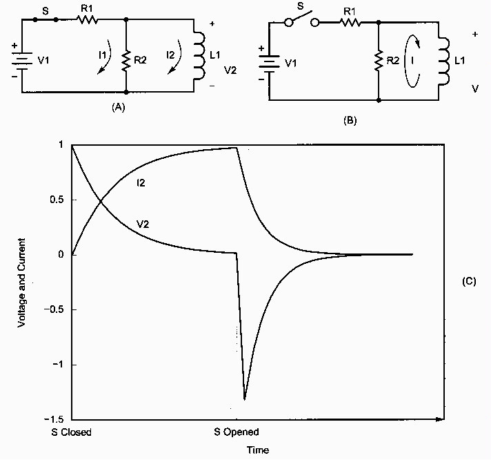
Fig 1 - Behavior of a switched ideal inductor. When S is first closed (A), currents flow through both the load (I1) and inductor (I2). Immediately after S is opened, current from the inductor continues to flow through the load in the same direction at the same value (B). (C) shows how I2 and V2 behave during switching.
If you start current flowing through an inductor by closing a switch (Fig 1A), the current will rise exponentially. Immediately after the switch is opened (Fig 1B), the current through the inductor continues to flow in the same,direction at the same value. The current decreases exponentially while the current flows through R2. The property that allows the voltage across an inductor to quickly change from positive to negative is the main property exploited in switching power supplies.
A Buck Regulator
The buck regulator is a variation on the classic choke-input supply. The output of a choke input supply is always the average value of the input waveform. In the case of a rectangular input waveform, the output voltage is simply the input voltage times the duty cycle of the input (Eq 1). It is possible for the input duty cycle to be any value between zero and 100%. The defining characteristic of a buck regulator is that the inductor provides current to the load during charging and discharging of the inductor.
![]()
Let's analyze the operation of a representative buck regulator. Our example regulator takes a nominal 12.6 V from a battery for a transceiver and creates 5.0 V for the digital logic. We'll assume that the logic draws 200 mA, which is the equivalent of a 25 Ω resistor as a load. The typical switching supply today uses a sample rate of 100 kHz or more. This allows us to use a very small value of inductor and a small value of output capacitor. The sample frequency of 100 kHz means that we will sample every 10 microseconds.
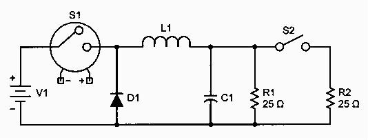
Fig 2-An idealized representation of our regulator.
Fig 2 is an idealized representation of our regulator. The regulator switch, S1, is an electronically controlled mechanical switch that opens and closes at the 100-kHz sample frequency. We start our analysis with the output voltage of zero and zero current flowing in the inductor (see Fig 3). During the first sample period, the majority of the inductor current flows into the output capacitor. The output voltage has not risen to 5.0 V yet, so the switch does not open (100% duty cycle). The same is true during the second sample period.
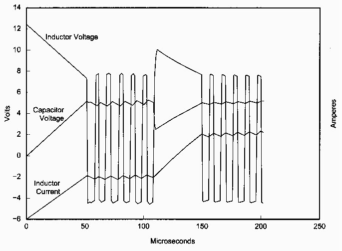
Fig 3 - An operational analysis of the regulator in Fig 2. See the text for details.
By the fifth sample period, most of the current of the inductor is flowing into the load resistor and the voltage has risen to the desired 5.0 V so the switch opens. When the switch opens, the current through the inductor continues to flow in the same direction into the load resistor. D1 is a commutating diode that allows the inductor current to continue to flow without significantly changing the effective resistance across the inductor. Without the diode, the energy stored in the inductor would be dissipated very quickly across the very high equivalent resistance of the switch. In other words, there would be an arc across the switch contacts.
The regulator has now reached the point where it is in regulation. When the sample period begins, the switch closes and there is 7.6 V (12.6 - 5.0) across the inductor. The inductor current increases until the switch opens. When the switch opens the voltage across the inductor decreases to the 5.0 V across the capacitor plus the 0.7 V drop across the diode. This lower voltage causes the inductor current to decrease at a lower rate than the charging current increase. The average current into the load resistance is easily calculated as the area under the triangular waveform. In our case, this average is 200 mA. Our assumption here is that the output RC time constant of the load resistance and filter capacitor is significantly longer than the 10 µs sample time.
Now we close S2 to model what happens with a large jump in load current. At first, the current in the inductor remains at the level of 200 mA. The additional current required by the second 25 Ω load resistor starts to reduce the voltage on the output capacitor. The regulator responds by keeping the switch closed through several sample periods so that the inductor charges up to 400 mA. You will notice that the ripple current is the same for 400 mA of output current as when delivering 200 mA (remember that this is a regulator with ideal components). We will look more closely at the non-ideal behavior of real components in real regulators in the next installment.
Step-Up Boost Regulator
Anyone who has ever worked on the high-voltage section of a TV or the ignition coil of an automobile is familiar with the mechanism that is the heart of a boost regulator. In general, a boost regulator operates by charging an inductor with current from a low voltage, low resistance source for a long period and then discharging the inductor over a much shorter period of time through a high resistance. The defining characteristic of a boost regulator is that the inductor provides current to the load only during discharging of the inductor.
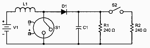
Fig 4 - This boost-regulator topology adds the voltage across the inductor to the input voltage for a boosted output.
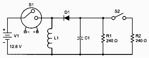
Fig 5 - This boost-regulator topology moves the switch between the supply and the inductor to reverse the polarity of the output.
There are two topologies for a boost regulator. One adds the voltage across the inductor to the input voltage to provide a boosted output voltage (Fig 4). If the switch is moved between the supply and the inductor (Fig 5), the polarity of the output voltage is reversed. Again, the commutating diode allows the current in the inductor to continue flowing when the switch opens. In this case, it also prevents current from flowing in the load while the inductor is charging.
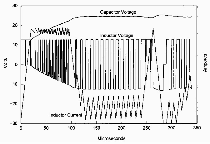
Fig 6 - An operational analysis of a voltage-boost regulator. See the text for details.
Fig 6 illustrates the operation of a voltage-boost regulator. Unlike the buck regulator, a boost regulator must have the duty cycle of the switch restricted to some value less than 100%. This is so because current is only delivered to the load when the switch opens. For our idealized example, we will limit the duty cycle to 95%. Again, we choose a sample frequency of 100 kHz. Before the control circuit can start operating, the commutating diode allows current to flow into the capacitor and the resistor charging it to the supply voltage (12.6 V). During the first sample period, the current in the inductor starts at 52 mA and rises at a rate controlled by the voltage across the inductor. Since the output voltage is 12.6, the control circuitry keeps the switch closed for the full 9.5 µs. The switch, S1, opens and current continues to flow in the same direction in the inductor. Now, however, the voltage across the inductor changes polarity and adds to the voltage of the power supply to charge the capacitor and deliver current to R1.
As the capacitor charges, the inductor current required tends to grow very large until the circuit is in control. For several reasons, it is necessary to limit the current in the inductor (1 A in our example) so that the control circuit will eventually be able to control the output voltage. In our example, the circuit must also keep the switch open allowing the inductor current to return to zero in order to compensate for the overshoot of the output voltage. Once the output voltage has stabilized at 24.0 V, the control circuit implements Eq 2.
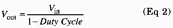
Again, we can look at what happens when a jump in load current occurs. We close S2, which places an additional 240 Ω of load on the circuit. The capacitor immediately starts supplying the additional current and its voltage starts to decrease. The control circuit responds by increasing the charge time of the inductor to bring the system back into stability. Again, this circuit is underdamped, so the voltage rises out of control and drifts back down to where the control circuit can use Eq 2 to control the output voltage.
Voltage-Inversion Boost Regulator
The other variation of the boost regulator is the voltage inverter. The operation of the circuit is similar to the step-up boost circuit. The switch and inductor trade places, and the diode is reversed from the boost configuration. We will again start our analysis with initial power on (see Fig 7). When the switch closes, current flows for the full 9.5 µs, charging the inductor. When the switch opens, the voltage across the inductor again reverses. This creates a negative output voltage across the capacitor and load. The control circuit continues to charge the inductor until the inductor current is sufficient to supply all of the load current during each sample period. The analysis of a change in load current is equivalent to that for the step-up boost regulator. Notice again that the inductor current is limited to allow the circuit to quickly come into control.
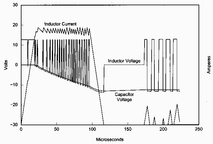
Fig 7 - An operational analysis of a voltage-boost inverter. See the text for details.
Basic Transformer Topologies
If you read textbooks on switching supplies, you will see transformercoupled supplies described as either buck or boost topology.
Buck converters are also called forward converters because the transformer operates as a true transformer. This means that while current is flowing in the primary, there is also current flowing in the secondary. Leakage inductance is an undesired side effect of the transformer operation.
A boost converter is also called a flyback converter, and the leakage inductance of the transformer is used to store the energy that is eventually delivered to the load. In flyback converters, the secondary current flows while the switch is off. It gets its name from the flyback circuit of a television horizontal-deflection system. In effect, the transformer of a flyback converter is really two inductors that share a common magnetic core rather than a true transformer.
It is very easy to get confused by the topologies when a transformer is involved. A buck regulator can only regulate a voltage to a lower value. A boost regulator can only create a higher voltage or a negative voltage. When a transformer is involved, both topologies can perform one or all of the voltage-conversion functions.
All off-line (hooked to the powermains) power supplies use either forward or flyback designs to isolate the load from the power lines using the inherent isolation of the primary and secondary windings of the transformer.
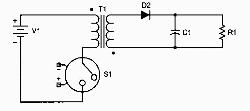
Fig 8 - A model of a flyback converter.
The Flyback Converter
Operation of the flyback converter is very similar to the operation of the boost converter. We vary the energy delivered to the load by varying the energy stored in the inductor. Since the energy is stored in the leakage inductance of the transformer, we intentionally control the size of this inductance.
Fig 8 shows a model of the flyback converter. Notice that the phasing is opposite to normal phasing of a transformer. The primary-side inductor is charged with energy while the switch is closed, and the energy in the core is transferred from the secondary-side inductor to the capacitor and load after the switch opens. This operation requires that the duty cycle be limited to a value less than 100 % as in a boost converter. The voltage across the primary inductor reverses (which forward biases the diode in the secondary) when the switch opens, and secondary current flows according to the transformer equation N1/N2 = I2/I1. The current flowing in the load circuit controls the voltage across the transformer windings. The voltage across the primary reverses polarity during energy delivery and this adds to the voltage of the input supply. The voltage across the switch is typically twice the input voltage.
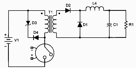
Fig 9 - A model of a single-switch forward converter.
The Single-Switch Forward Converter
Fig 9 shows a single-switch forward converter. Notice that a major difference from the flyback converter is the phasing of the transformer windings. This converter delivers energy to the filter during the time the switch is closed. We use the almost rectangular shape of the voltage across the primary and secondary of the transformer to vary the amount of energy delivered to the filter and load circuit. The output voltage is controlled by the averaging effect of the low-pass filter. We must provide a controlled path for the current in the leakage inductance to flow once the switch opens, since the current cannot immediately return to zero. This path is provided by D3 and D4 in Fig 9. There are various other ways to control the path of the current discharge. We will look closely at those in the design section. The voltage reversal that discharges the current adds with the supply voltage. The consequence is that the peak voltage across the switch is typically twice the input voltage.
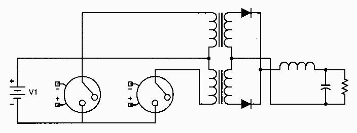
Fig 10- A model of a push-pull forward converter.
The Push-Pull Forward Converter
Fig 10 shows a push-pull forward converter. This circuit is identical to a push-pull audio or RF circuit except that the signals are rectangular waves. This circuit uses the core to full advantage because the current flowing in opposite windings creates a net zero dc current flow for the core. This allows the full magnetic capability of the transformer core to be utilized. This circuit has the advantage that the drive circuitry for the switches is relatively simple, since both switches are referenced to the common of the input supply. Each switch must withstand twice the input supply voltage. The disadvantage of this circuit is that the transformer primary requires two balanced windings. The 1969 ARRL Handbook portable/emergency chapter shows a circuit utilizing self-excited push-pull forward converters. There are two disadvantages to selfexcited converters: ensuring proper starting and reproducing the saturation characteristics of the magnetic circuits from supply to supply.
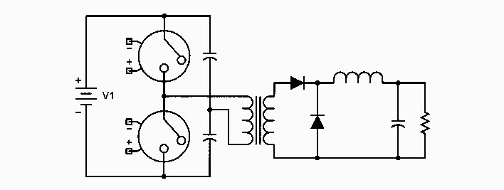
Fig 11 - A model of a half-bridge forward converter.
The Half-Bridge Forward Converter
Fig 11 shows a half-bridge forward converter. This circuit is essentially the same as a totem-pole audio output stage. The difference being that the waveforms are high-frequency square waves instead of audio signals. This configuration also has the advantage that the current flows in opposite directions during opposite cycles, so the transformer core has a net zero dc current flowing in it. The transformer primary has one-half of the input voltage across it. Each switch need withstand only the input supply voltage. This circuit is capable of higher power levels than the singleswitch converter for equal-size comswitch converter for equal-size components. The disadvantage is that the drive circuitry for the top switch must be isolated from the input-supply common connection.
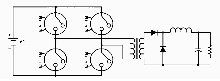
Fig 12 - A model of a full-bridge forward converter.
The Full-Bridge Forward Converter
Fig 12 shows a full-bridge forward converter. This circuit replaces the capacitance voltage divider with a second set of switches. Again, there is a net zero de current in the primary so the full capability of the transformer is used. The full input supply voltage is placed across the transformer primary. Each switch must withstand only the input supply voltage. In this circuit, we need two isolated drive circuits for the top switches. The full-bridge converter gives the highest possible output power for a given size of components at the cost of four switches and two isolated drive circuits.
Next Installment
The next installment will cover the characteristics of real magnetic components and guidelines for how to design a transformer or filter inductor.
Acknowledgements and References
I thank the folks at Linear Technology, who made a special version of their SwitcherCAD program to assist in the drawing of the schematics in this article. SwitcherCAD is available free on the Linear Technology Web site. You can find short application notes on switching power-supply design that complements the information in these articles in the application note sections of the Web sites for Linear Technology and Maxim Semiconductors (https://www.analog.com/en/index.html).
WD5IFS, wd5ifs@arrl.org