Home - Techniek - Electronica - Radiotechniek - Radio amateur bladen - QST - High-gain voltage-controlled transistor amplifier
High-gain transistor amplifier designs are often relatively unstable. In addition, most of these circuits require excessive power. It is possible to build an amplifier combining high gain with stability and low power consumption, using the circuit in Fig. 1. This amplifier's gain is controlled by an external reference voltage. Closed-loop gain is about 15,000.
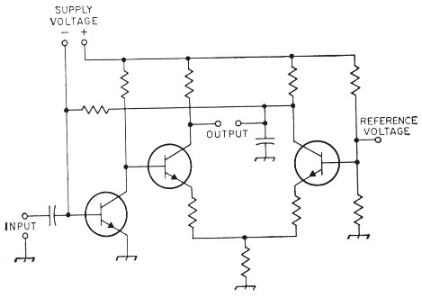
Fig. 1. Simplified circuit diagram of the high-gain amplifier. Resistors values will depend on the transistors used and available supply voltage. The transistors are, from left to right, Q1, Q2 and Q3. All are silicon n.p.n. types with betas greater than 100.
The gain of the amplifier stage, Q1, is stabilized by using a difference amplifier circuit, Q2 and Q3, to sense and correct changes in Q1's operating point. The a.c. gain of Q1 is controlled by its d.c. operating point. This d.c. operating point is controlled by the difference amplifier, Q2 and Q3i through the feedback loop Loin the collector of Q3 to the base of Q1. Varying the reference voltage to the base of Q3, therefore, varies the a.c. gain of the amplifier.
The overall stability of this circuit depends on the use of quality components and transistors with betas greater than 100.
NASA Tech Brief 65-10138