Europe Card Bus
The ECB-bus was defined in 1984 by the german company KONTRON.
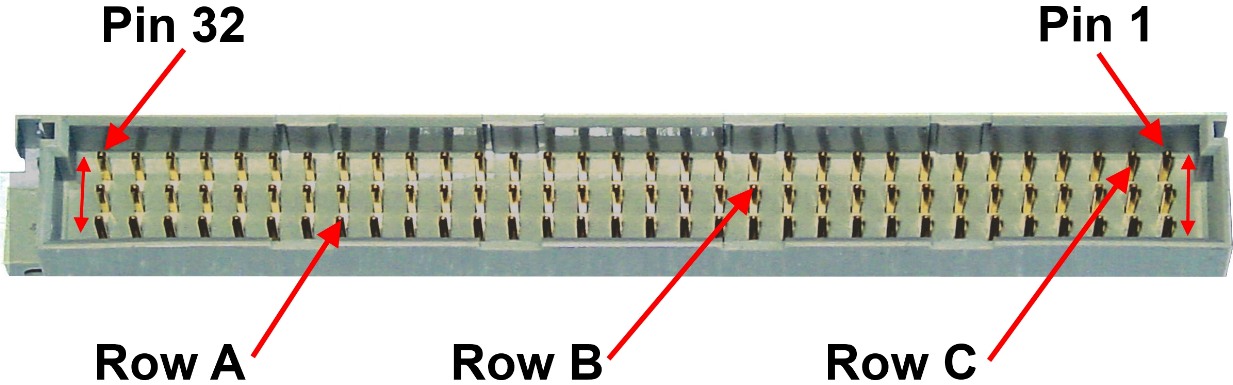
It was defined for the 100 × 160mm-europa-card and used 2 × 32 pins of a 3 × 32-pin-connector (row a and c).
Later the third (middle) row of pins was defined for additional signals used in 16-bit-systems. This extended bus uses all 3 × 32pins.
Physical format
Mechanically, the ECB is usually implemented as a backplane circuit board installed in a 19-inch rack chassis. ECB cards have 3U Eurocard format (100 mm × 160 mm).
Connector
Use two or three-row versions of DIN 41612 connectors, 0.1" pitch. Original Kontron ECB, supported 64 pins, using "a" and "c" rows, "b" row tied to "C" row. ECB boards are NOT compatible with STE-bus or VME-bus P2 connector (while STE-bus does not use the "b" column; VME does define specific signals on the "b" row).
 Card connector male.
| Row A | Row C | ||||
|---|---|---|---|---|---|
| Desciption | Name | Pin | Pin | Name | Desciption |
| +5 volts DC | +5 V | a1 | c1 | +5V | +5 volts dc |
| Data line bit 5 | D5 | a2 | c2 | D0 | Data line bit 0 |
| Data line bit 6 | D6 | a3 | c3 | D7 | Data line bit 7 |
| Data line bit 3 | D3 | a4 | c4 | D2 | Data line bit 2 |
| Data line bit 4 | D4 | a5 | c5 | A0 | Address 0 |
| Address 2 | A2 | a6 | c6 | A3 | Address 3 |
| Address 4 | A4 | a7 | c7 | A1 | Address 1 |
| Address 5 | A5 | a8 | c8 | A8 | Address 8 |
| Address 6 | A6 | a9 | c9 | A7 | Address 7 |
| CPU-wait | WAIT/ | a10 | c10 | ||
| Bus request | BUSRQ/ | a11 | c11 | IEI | interrupt enable in |
| a12 | c12 | ||||
| +12 volt DC | +12V | a13 | c13 | ||
| -12 volt DC | -12V | a14 | c14 | D1 | Data line bit 1 |
| -5 volt DC | -5V | a15 | c15 | ||
| 2x clock | 2PHI | a16 | c16 | IEO | interrupt enable out |
| a17 | c17 | A11 | address 11 | ||
| address 14 | A14 | a18 | c18 | A10 | address 10 |
| a19 | c19 | ||||
| first cycle | M1/ | a20 | c20 | NMI/ | not maskable interrupt |
| a21 | c21 | INT/ | normal interrupt | ||
| a22 | c22 | WR/ | write cycle | ||
| a23 | c23 | ||||
| a24 | c24 | RD/ | read cycle | ||
| a25 | c25 | HALT/ | cpu stopped | ||
| a26 | c26 | ||||
| in/out request | IORQ/ | a27 | c27 | A12 | address 12 |
| refresh cycle | RFSH/ | a28 | c28 | A15 | address 15 |
| address 13 | A13 | a29 | c29 | PHI | clock |
| address 9 | A9 | a30 | c30 | MREQ/ | memory request |
| bus acknowledge | BUSAK/ | a31 | c31 | RESET/ | cpu reset |
| signal ground | GND | a32 | c32 | GND | signal ground |
Note: / = Active Low