New RF transistors with improved noise figure and gain
New RF transistors with higher gain and reduced noise factor have resulted from the further developments in manufacturing technologies. These developments include improved methods in optical lithography to define the extremely fine structures, in reactive ion etching when these structures are transferred to the chip and also in doping techniques.
The BF988/BF998 UHF MOS tetrodes with a 1-µm gate length give a 1-dB noise figure with 20-dB gain at 800 MHz when used in controlled prestages in high quality TV tuners.
For the same application in the satellite IF band of 950 to 1750 MHz the CF139/ CF739 gallium arsenide tetrodes are ideal. Because of the high electron mobility in GaAs, these still have a 1.8-dB noise figure with 17-dB gain at 1750 MHz.
The first types of the new silicon SHF transistors with improved characteristics are the BFQ82 and BFR193/BFP193 NPN bipolar transistors for use in radio links and antenna wideband amplifiers.
BF988 and BF998 MOS tetrodes
Early in 1988 Siemens introduced the BF988/BF998 MOS tetrodes, where for the first time in volume production the gate length has been reduced from 2 µm to 1 µm. In comparison to the BF966S and BF996S tetrodes, which were introduced some time ago, the BF988 and BF998 achieve significantly better values of transconductance, capacitance and noise figure. They have been developed for use in controlled prestages of high quality TV/VCR tuners with a tuning range from 50 MHz to 1 GHz.
Modern TV tuners must have optimum noise and large signal characteristics to qualify for use in the latest developments such as CATV/hyperband receivers. Key devices in the construction of these tuners are MOS tetrodes, as these devices provide the required prestage gain.
In selecting suitable tetrodes, questions of economy must be considered as well as the ordinary technical specifications such as low capacitance or high transconductance. Therefore, with mass-produced equipment frequencies below 1 GHz, components manufactured in the well proven silicon technology still have preference over GaAs devices. Siemens meets both the technical and the economic requirements with the new MOS tetrodes BF988 (X-Plast package) and BF998 (SOT-143 package). In both packages (Fig. 1) the same chip manufactured in Si planar MOS technology (Fig.2) is used.
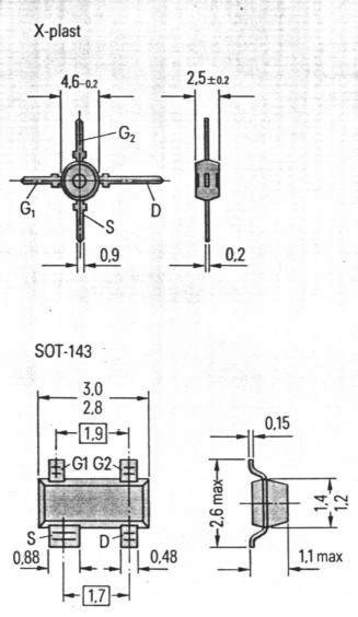
Fig. 1 X-Plast and SOT-143 packages are used for the 1 µm MOS tetrodes BF988 and BF998 as well as for the GaAs MESFET tetrodes CF139 and CF739
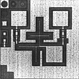
Fig. 2 The MOS tetrode chips with 1 µm gate length for controlled prestages of UHF tuners
The new MOS tetrodes are based on the specifications of the BF966S and BF996S UHF transistors already introduced, but have one major advantage over the existing types. While with the earlier types 2 µm was the channel length of Gate 1, with the new types 1 µm can be obtained through improved manufacturing techniques (Fig.3). This reduction improves the high-frequency characteristics of the UHF tetrodes. With small gate lengths the ratio of transconductance to input capacitance rises. The higher this ratio, the higher is the frequency at which the noise figure finally increases.
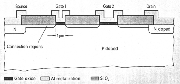
Fig. 3 Cross section of the BF988 and BF998 tetrode chip
The differences between the RF data of the new BF988BF998 MOS tetrodes and that of the well proven BF966S/BF996S transistors are shown in Table 1.
| Characteristics | BF966S, BF996S | BF988, BF998 | CF139, CF739 | |
|---|---|---|---|---|
| Transconductance gfs | 18 | 24 | 30 | mS |
| Gate-source capacitance Cglss | 2.3 | 2.1 | 1 | pF |
| Figure of merit gfs/Cglss | 7.8 | 11.4 | 30 | mS/pF |
| Noise figure(800 MHz) | 1.8 | 1 | 0.8 | dB |
| Gain (800 MHz) | 18 | 20 | 22 | dB |
| Noise figure (1750 MHz) | 3.3 | 1.8 | dB | |
| Gain (1750 MHz) | 12 | 17 | dB | |
| Typical operating point: | ||||
| UDSS | 15 | 8 | 5 | V |
| UG2S | 4 | 4 | 2 | V |
| Gate length | 2 | 1 | 1.5 | µm |
| Gate width | 1250 | 1100 | 640 | µm |
| The current Idss = 10 mA is set with UG1S; depending = on Idss a UG1S is needed of: | about 0 | about 0 | about -1 | V |
Apart from shortening the gate length, a number of other development steps in the production process ensure reliable operation of the new devices. The individual steps have diffused source and drain connection regions with such a low penetration depth that the channel length of Gate 1 is not shortened. Aluminum is used as gate metalization as it keeps conducting path resistance fairly low, thus minimizing its effect on the RF noise figure. Moreover, the gate oxide is applied in a thin layer to ensure the required transconductance. A very important aspect in this context is the overload rating, as electrostatic discharges may destroy these MOS devices. Gate protection diodes form a safety barrier. A new design gives a very low resistance during a voltage breakdown and protects the gate oxide from excessive field strengths.
Another technique further improves the reliability of the new UHF MOS tetrodes. The current handling capability particularly during drain-source breakdown is guaranteed by keeping the doping and the penetration depth in the drain and source areas within extremely tight tolerances.
GaAs MESFET tetrodes CF139/CF739
At frequencies above 1 GHz, a significantly higher gain and a lower noise figure justify the use of the GaAs tuner tetrodes CF139/CF739 despite the high cost of GaAs compared to silicon. They are supplied like the MOS tetrodes in X-Plast (CF139) and SOT-143 (CF739) packages.
In TV satellite communications, for example, the RF signal in the 11.7 to 12.5 GHz band is frequency converted close to the antenna down to the IF band 950 to 1750 MHz. Here the cable losses are low enough that the signal can be sent through ten meters or more of cable to the tuner of the indoor unit.
CF139/CF739 transistors allow tuners to be built with controlled input stages similar to those of TVNCR tuners in the UHF band(1).
Table 1 compares the most important data of the CF139 with that of the MOS tetrodes BF988/BF998. The higher electron mobility in gallium arsenide results in a transconductance of 30 mS with a smaller gate width than with the BF988, i.e. with a reduced input capacitance of only 1 pF. The gain in the UHF region is 22 dB (2dB more than with the MOS tetrode) and at 1.75 GHz it is still 17 dB. As can be seen from Table 1, the GaAs MESFET can be operated from smaller supply voltages than the MOSFET types(1).
The chip of the new GaAs tetrodes (Figs.4 and 5) has integrated NIN diodes at the gate inputs as protection against electrostatic discharges. The CF139 and CF739 are therefore comparable with the MOS tetrodes described above in terms of handling. The tetrodes are produced in the new GaAs MESFET technology with resistive and Schottky contacts produced by different implantation of the aAs areas below and with the same sequence of metal layers. A description of the process has been published under the name "Double Implantation, One Metalization" technology (DIOM)(2). The DIOM technique has major benefits: the critical metalization process is carried out only once. Gate-drain and source-drain metalization are defined on the same mask level and have precise spacings. This results in a high yield and high reliability.
Fig. 4 The GaAs MESFET tetrode chips for use in controlled tuner prestages of satellite receivers (950 to 1750 MHz)
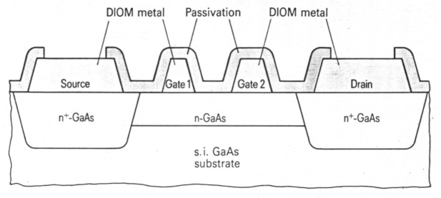
Fig. 5 Cross section of the CF139 and CF739 GaAs MESFET tetrode chip
Moreover, the usual recess etching of the gallium arsenide under the gate is not applied in this process. The GaAs surface remains plane. Silicon nitride passivation provides the final protective coating against environmental effects.
BFQ82 and BFR193/BFP193 bipolar transistors
The new SHF transistor chip is supplied in three different packages (Fig.6): the BFR193 in the SMD plastic package SOT-23, the BFP193 in the SOT-143 and the BFQ82 in the CEREC package.
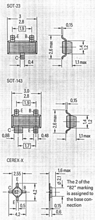
Fig. 6 The new bipolar transistor chip is mounted in SOT-23 (BFR193), SOT-143 (BFP193) and CEREC (BFQ 82) packages
It is ideal for use as an oscillator in radio link applications up to 6 GHz and as a wideband amplifier including IF amplification, as well as in wideband antenna amplifiers for high gain and low noise. The progress achieved with this transistor in its high frequency characteristics arises from the improvement in its vertical and lateral structures.
With bipolar transistors the high frequency properties are determined by the cut off frequency fT and the feedback time constant rb (rb = base resistance, formed by contact resistance, connection path resistance and the internal base resistance; Cc = collector capacitance). With the new transistors an increase of fr from 5 to 7 GHz has been achieved by optimizing the doping process (vertical geometry).
In addition, the use of improved projection lithographic equipment leads to a resolution below 1 µm in production. This allows new design rules (Figs. 7 and 8) for the lateral geometrical structure of the transistor chip to be introduced, giving a smaller feedback time constant. The pitch of the elementary cell - in other words the spacing of two neighboring base contacts, which together enclose an emitter, could be reduced to 5 µm (Cc is proportional to the area of the transistor's elementary cell).
Fig. 7 The new bipolar transistor chips for amplifier and oscillator applications in VCRs and TV sets and in telecommunications
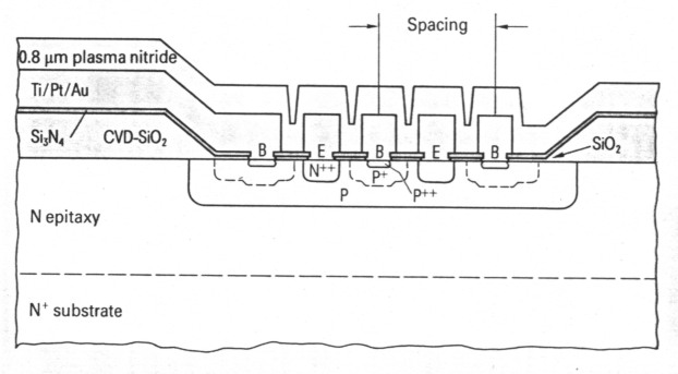
Fig. 8 Cross section of the BFQ82, BFR193 and BFP193 bipolar transistor chip
A uniform emitter width of about 0.8 µm is obtained (the internal base resistance is proportional to the emitter width). This explains the improved data of the new BFR193 transistor (in SMD package SOT-23). Comparison with the data of the BFR93A, which has almost the same size and represents the previous state of development, is shown in Table 2.
| Characteristics | BFR93A | BFR193 | |
|---|---|---|---|
| Emitter width | 1 | 0.8 | µm |
| Width of elementary cell | 8 | 5 | µm |
| fT | 5.7 | 7 | GHz |
| fT maximum at Ic | 50 | 50 | mA |
| rb | 9 | 5 | a |
| C12e (5 V, 1 MHz) | 600 | 670 | fF |
| fmax | 6.5 | 9.1 | GHz |
| Noise figure at 800 MHz | 1.6 | 1.2 | dB |
| Noise figure at 2 GHz | 3.3 | 2.3 | dB |
| The fmax values of the new transistor chip in the CEREC package (BFQ82) more suitable for microwave applications lie around 11 GHz. | |||
Automatic alignment gives a higher overlay accuracy of the subsequent mask so that
- the distance of the base contact region from the emitter edge (proportional to the base connection path resistance) is reduced and
- overlapping of the metalization over the window can be guaranteed, giving a positive effect on reliability.
Hence the high reliability of Siemens bipolar high-frequency transistors (chip hermetically sealed by thick silicon nitride passivation(3) obtained by the hi-rel application of wideband cable transmission repeaters, also applies to the BFQ82. In the hermetically sealed CEREC package the transistor has an ideal cost/performance ratio for professional applications and thus extends the well proven range of BFQ70 to BFQ77 high-frequency transistors.
With 25 emitters of, each 25-pm long, its maximum fT is at about 50 mA. Hence the BFQ82 is a general purpose transistor for front end and driver stage applications.
For particularly low current or highly linear applications further transistors are in the development stage, following the design principle of the BFQ82.
References
- Reuschle, R.: GaAs-MESFETs in Tunervorstufen. Funkschau 13 (1988), pp. 48 to 49
- Pettenpaul, E.: State-of-the-art of MMIC technology and design in West Germany. 1987 IEEE MIT Int. Symp. Dig.: Las Vegas, pp. 763 to 766
- Henning, W.; Weidlich, H.; Werner, K.: Qualität und Zuverlässigkeit der ChiptransistorHybridschaltung für das 60-MHz-Koaxialkabelsystem. Siemens Forsch.- u. Entwickl.-Ber. Bd. 9 (1980) No. 3, pp. 151 to 157
Karl Platzöder, Herbert Weidlich.