A new pulsed bi-phase digital communications system 1
19.2 kB in a 3 kHz bandwidth? Read on to see how!
Amateurs have traditionally been the forerunners of radio progress. They have pioneered short waves in the 1920s, and single signal superhets and single sideband in the 1930s and 1950s. Well, the same pioneering can be done in digital telecommunication techniques!
This article describes a new technique of pulsed, bi-phase shift-keyed (BPSK) modulation that opens up the new field of narrow band digital radio. The system tailors new methods to fit the requirements of a narrow band system, and abandons the conventional method of 180° sinusoidal phase reversals, which produces a large number of sidebands and a consequent wide frequency spectrum of the signal. This wide bandwidth has been accepted in the past as a necessary evil of digital communication.
Small phase deviation
The key elements in the new pulsed BPSK modulation system are:
- the very small phase angle deviation, and
- the nanosecond linear transient of the phase modulation.
Hund analyzed the sidebands generated by small phase deviations. At small phase angles of 0.2 radian (11.5°) or less, only two main sidebands, similar to AM sidebands, are generated. The modulating frequency f determines the sideband spacing from the carrier. The width of a sideband is the the modulating frequency variation, as in AM. Each side-band contains an equal amount of information. This allows PSK transmission on a single sideband (SSB) by using a small deviation angle and a bandpass filter to pass one sideband and reject the carrier and the other sideband. The width of this single side-band is reduced by a novel coding method that uses pulsed phase deviations of 0.02 radians (1.2°) to represent the digital information. The novel coding incorporates a timing pulse in every bit, which provides a coherent clock at the receiver enabling synchronous operation.
Synchronization
How does a receiver demodulate this single sideband without a reference carrier? By pulse coding the deviations to allow polarized pulsed detection in a digital phased locked loop (PLL) demodulator system. Binary "one" is encoded as a brief pulse of a leading phase angle at the start of a clock period and a brief pulse of a lagging phase angle at the middle of this clock period. Binary "zero" is encoded only as a brief pulse of a lagging phase angle at the middle of a clock period. This coding thus provides a timing pulse at the middle of every bit for directly transmitting the clock.
The phase deviations arise from the transitions at the rising and falling edges of the rectangular phase modulating pulses approximately Ills long. The phase angle deviation during the nanosecond rise and fall of the modulating pulse is approximately 0.02 radian or 1.2°. The sine wave carrier is phase modulated during a very small portion of a single carrier cycle when using this method, so modulation products occupy a very small frequency spectrum.
TX Modulator
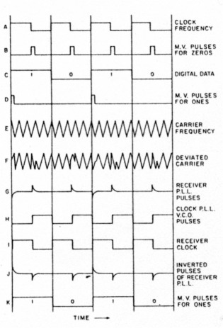
Figure 1. Waveforms used in the pulsed BPSK mien/ and their timing relationships.
The wave shapes used in this system are shown in Figure 1. Figure 2 shows a block diagram of the transmitter's simple modulation system.
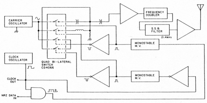
Figure 2. Transmitter block diagram.
A sine wave oscillator feeds a one-volt signal through the quad bilateral switches to separate L and C phase shift circuits when these switches are pulsed. The sine wave remains unshifted during the intervals between the digital bit pulses. The square wave clock oscillator circuit drives an inverter, which in turn drives a monostable multivibrator (M.V.) to produce a "zero" modulating pulse at the middle of every clock cycle. This pulse drives a switch to connect the L phase shift circuit to produce a lagging phase angle.
The NRZ data input, clocked by the clock oscillator, drives one side of the AND gate while the clock frequency drives the other side. When a digital "one" appears at the gate, the AND gate drives a second monostable M.V. to produce a "one" modulating pulse at the start of a clock cycle. This pulse drives a switch to connect the C phase shift circuit to produce a leading phase angle.
Inverters driven by the pulses open the switches, which transmit the carrier directly for the pulses' duration. When no pulses are present at the inverter inputs, the inverters drive the two switches closed to transmit the carrier directly to the load R without phase shift. The load resistance is coupled to a high impedance input amplifier, the output of which drives a frequency doubler.
At this point, there is a carrier with two sidebands present. The sidebands are about 1 % of the carrier amplitude. A crystal single sideband filter selects the upper sideband, and an amplifier feeds the narrow single side-band to the antenna.
At the receiver
Here, the SSB sine wave signal at a 455 kHz intermediate frequency (IF) is amplified to make it a square wave at the logic level (Figure 3). The square wave is further squared by a Schmitt trigger, and its leading edge is compared to the leading edge of the PLL voltage-controlled (VCO) square wave in the digital phase comparator of a well-damped PLL by RCA. The signal square wave input is also compared in a second digital phase comparator with the PLL VCO. The second digital phase comparator gives a positive output pulse for a lagging phase angle input, and a negative pulse for a leading phase angle input. This allows unambiguous identification of digital "ones" and "zeros" with out a reference carrier, not possible in previous PSK systems.
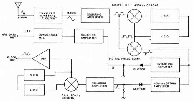
Figure 3. Block diagram of the pulsed BPSK demodulator
The digital PLL locks on to the frequency of the bit stream. An inverting amplifier then amplifies the negative output pulses denoting binary ones from the second phase comparator. A diode clipper removes the negative portions of the signal. The positive "zero" pulses are amplified to a square wave at the logic level. A PLL digital phase comparator then compares these pulses with the square wave output of the VCO at the clock frequency but 180° out of phase. An inverter brings the VCO output into phase and feeds the clock output terminal, thus furnishing a coherent clock for the receiver.
Bandwidth limits
With this encoding method for a clock frequency f, a string of "zeros" gives the inner sideband boundary as fΔθ, where f is the modulating frequency, and Δθ is the phase deviation angle from the center frequency of the carrier frequency F. The outer sideband boundary is 2fΔθ, for a string of "ones," which have two pulses per clock cycle. Then 2f-fΔθ = fΔθ, the width of the sideband. As modulation takes place during the nanosecond rise and fall times of the pulses used, f is effectively multiplied by two. Since the deviation used is only 0.02 radian, and there are 2n radians in a cycle of the carrier frequency, this results in (2 × 20,000 × .02) ÷ 6.28 = 127 Hz bandwidth for a clock frequency of 20 kHz.
Prototype characteristics
A working breadboard prototype has been operated at a carrier frequency of 21.4 MHz and a clock frequency of 19.6 kHz, an adequate, speed for digital telephony or transmission of computer data. These benefits come, however, by sacrificing the high speed performance of the conventional 180-degree phase shift systems. It's a trade-off of speed for economy, simplicity, synchronous operation, and bandwidth. The experimental system is capable of synchronous transmission and reception of 6-bit digital telephony in a bandwidth formerly associated with CW transmission!
The breadboard system has the following characteristics:
| Transmitter | Carrier frequency 21.388 MHz |
| Upper side band | 21.400 MHz |
| Clock frequency | 19.6 kHz |
| Digital input RZ or NRZ | 12V data |
| Power output | 10 mW |
| Receiver | Hammarlund HQ-101A with 455 kHz IF 0.2V P-P |
| Receiver bandwidth | 3 kHz |
| Demodulator accepts | 455 kHz 0.2V P-P sine wave |
| Demodulator output | RZ or NRZ 12V data, 12V clock |
System construction
I bread-boarded the experimental system using standard Radio Shack H276-174 2" x 6" experimenter boards, with the ends trimmed off to fit the bottom of standard 3" x 5" x 2" aluminum boxes on top of a piece of 1/4" thick corrugated carton material, and glued in place. The carton material reduces capacity to ground.
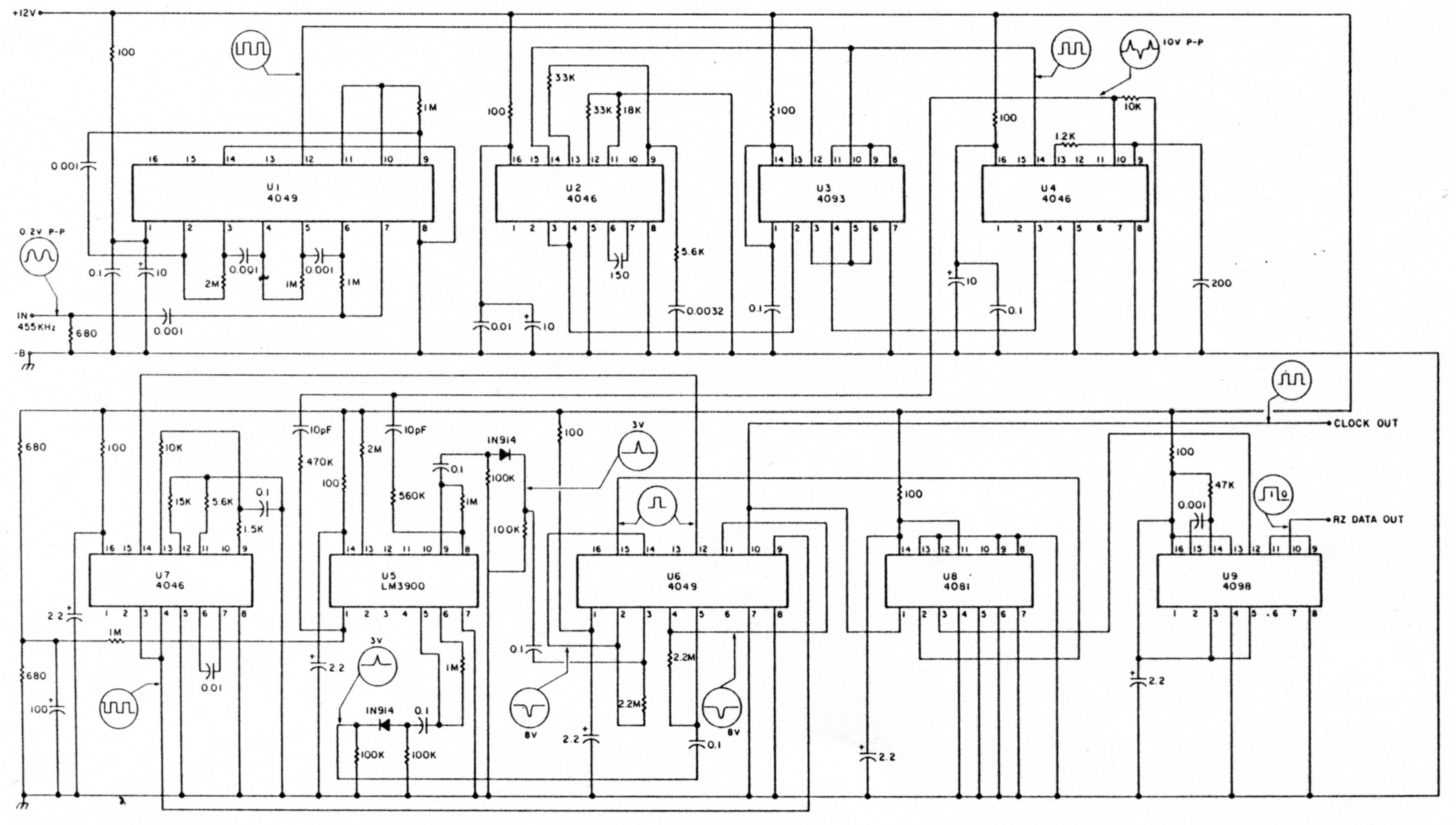
Figure 4. The transmitter schematic. It provides a pulsed BPSKoutput on 21.4 MHz.
Figure 4 is the schematic diagram of the modulator and carrier generator units. Q1 is a standard crystal oscillator for crystal Y1, which has a frequency of 10.694 MHz. Q2 is a source follower and delivers a sine wave at about 1 volt to the 1.2kΩ resistor at terminal 1 of U1 a quad bilateral switch.
Narrow pulses from U4 drive control terminals 5, 6, 12 and 13 of U1. When terminals 8 and 9 of U4 are driven by a narrow positive pulse from pin 10 of one shot M.V. U5. Pin 6 of U1 receives this pulse and closes the transmission gate between pins 8 and 9, which feeds carrier voltage from terminal 1 to C1 and R1, shifting the phase of the carrier to a leading phase angle. The complementary pulse from inverter pin 10 of U4 at the same time opens the transmission gate between pins 3 and 4 of U1, which had been closed to transmit the carrier directly to R1. Also, when pins 12 and 13 of U1 are driven by a narrow positive pulse from terminal 6 of U5, pin 12 of U1 receives this pulse and closes the transmission gate between terminals 10 and 11, which feeds carrier voltage from pin 1 to L1 and R1, shifting the phase of the carrier to a lagging phase angle. The value of R1 determines the phase angle.
The complementary pulse from inverter #11 of U4 at the same time, opens transmission gate between pins 1 and 2 of U1, which had been closed to transmit the carrier directly to R1. When no pulses appear at pin 6 and 12 of U1, as in the time between pulses, gates between 1 and 2, 3, and 4 are closed by the inverters, so the carrier appears across R1 without any phase shift. The dual M.V. at U5 gives "one" pulses from pin 10, and "zero" pulses from #6, 1µsec wide.
The clock oscillator U2 has a square wave output at pin 10, with a complementary output at #11. Frequency divider U3 is driven at pin 1 by the complement at pin 11 of U2 and pin 12 is a divide-by-two output of the clock frequency. The square wave output of #12 of U2 is inverted at terminal 3 of U4, and can then serve as a test program of alternate ones and zeros when applied to terminal 2 of U6 by switch SW1.
The clock frequency square wave from pin 11 of U2 is sent through three AND gates of U6 to delay its leading edge until later than the trailing edge of the "one" pulse at pin 2 of U6. This delay prevents a false "AND" output from pin 3. A small capacitor might be necessary from #9 of U6 to ground to increase this delay in cases where clocked data signals are delayed excessively by the digital processor in use.
Pin 5 of U5 is driven by the trailing edge of the clock pulse to produce "zero" pulses from #6 at the middle of each clock cycle. Terminal 12 of U5 is driven by a pulse from pin 3 of U6 when the rising edge of a "one" pulse and the rising edge of the clock pulse are "ANDed" at pin 3. In this manner, a "one" pulse is delivered at #10 of U5 and a "zero" pulse is delivered at #6 of U5 at the proper times to accomplish the coding of the phase deviations of the carrier.
Output coupling
The carrier voltage on R1 drives a source follower Q3, with high input impedance, and its low impedance output drives the amplifier Q4, which in turn drives the frequency doubler Q5. Output tank L2 C2 is tuned to the second harmonic of oscillator Q1. A few turns on L2 serve to couple to the output terminal at low impedance.
The output terminal and ground are connected by twisted pair to the input of the single sideband filter unit shown in Figure 5. The six-pole crystal filter centered at 21.400 MHz has a bandwidth of 12 kHz and drives a high impedance input amplifier Q1. Amplifier Q2 drives the output stage Q3. Output tank L1 C1 is tuned to 21.400 MHz. A few turns on L1 are used to couple to a few feet of antenna wire adequate for the 10-milliwatt experimental transmissions.
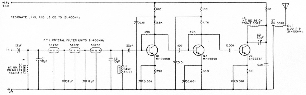
Figure 5. Filtering and antenna coryding details. Test transmissions generated approximately 10 mW output.
K6HH, William Hotine.