10 GHz RF Preamp
A building block toward a complete 10 GHz transceiver system
Construct an amplifier for the 10 GHz microwave band? How about 18 dB gain and 3 dB noise figure at 10 GHz? Does it sound impossible? Well, it isn't! San Diego Microwave Group members have constructed several of these amplifiers and all have worked quite well. Thanks to Clark Bishop WB4PQD, who designed this stable, high performance, dual-mode amplifier for 10.12 GHz, and who is allowing us to publish the design for amateur use.
Preamp Construction
The amplifier described here has been used as a receiving preamplifier and as a transmit amplifier, with appropripte RF relay switching. Construption of this amp is somewhat%delicate due to its small printed circuit board and components. The finished PC board is 1½" by 1" (see Photo A).
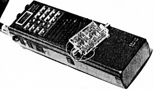
Photo A. Close-up showing the 10 GHz preamp on top of an IC-02 battery box for size comparison. The amplifier uses two MGF-1402s and boasts only 3 dB noise figure and 18 dB gain.
Mitsubishi's low-cost (about $15 each) Gallium Arsenide Field Effect Transistor (GaAsFET) MGF-l402 is central to the preamplifier's design. It has gold metalization strapping over the ceramic case, connecting the two strip line opposed source leads. Most importantly, this metalization reduces the total inductance of the source leads . necessary for good operation at 10 GHz. When ordering, be sure to specify the full gold metalization over the case connecting the source leads together.
In other designs, the emitter or source leads are bent down and over to connect to the rear ground foil. At lower frequencies, this works well, but at frequencies above 5 GHz, a very small inductance in the leads will give low gain and the amplifier may become useless. Lead length is critical for proper operation. See Figure 1 for the schematic and parts placement.
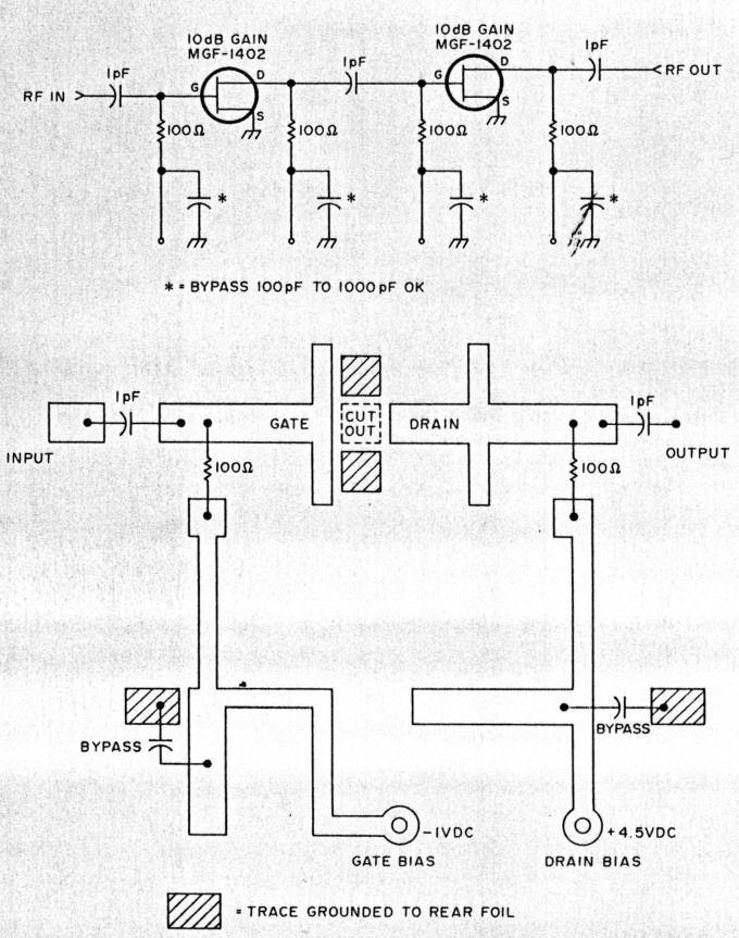
Figure 1. 10 GHz preamp schematic and parts placement diagram.
The Teflon PC board is 0.031" thick, with a dielectric constant of 2.5. You will need Teflon stock because other materials will not perform at microwave frequencies. If you can not find any Teflon, or just don't wish to make our own, I will provide the etched PC boards and/or a minikit of parts.
The amplifier is a two-stage device requiring a small power supply with negative bias and positive drain. Current demands are light. The external power supply that I built furnishes a bias of -1 volt DC and drain voltage of +4.5 volts. You could use an AA battery for bias and an adjustable regulator for the drain voltage (see Figure 2).
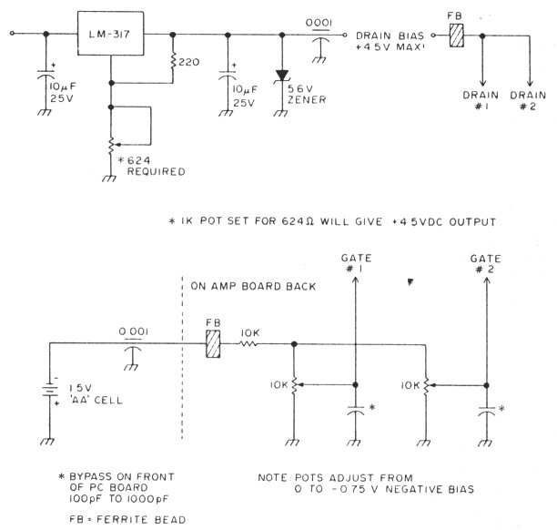
Figure 2. Power supply with battery for the 10 GHz preamp.
Building the Power Supply
I decided to build a power supply that provided sequencing protection, as Ray W6AMD suggested. By putting a series pass transistor in the positive input circuit, the positive voltage will not activate until the bias supply is operating at full potential (see Figure 3). I have used this protected power supply for months, and it has proven reliable. It runs from a 12 volt supply. The negative power supply is enclosed in a small 24-pin DIP package and looks much like a large EPROM. The transformer-isolated power supply is regulated to -9 volts with 40 mA of current available.
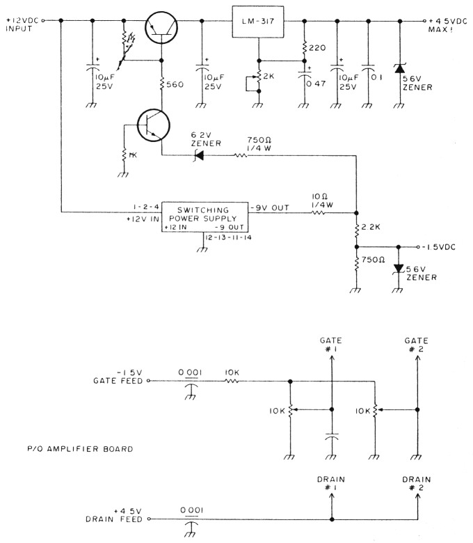
Figure 3. Power supply for preamp. Supply provides sequencing protection. The schematic below the power supply schematic shows where the power supply leads attach to the amp board.
We only need a few mA, so the power supply loafs in this application. Part of the negative supply is voltage divided to the -1.2 volts to feed the gate bias circuitry. This requires very little current. The main -9 volt output is fed to a series current limiting resistor in series with a 6 volt zener diode, which in turn feeds the emitter of a 2N2222 NPN transistor.
Tie the collector of the 2N2222 to the base of the 5 Watt dissipation PNP pass transistor which controls the input of the LM-317 positive adjustable regulator. When you apply + 12 volts to the power module, the negative power supply turns on, producing -9 volts output. This negative voltage passes through the 2N2222 switching transistor, and turns on the base of the pass transistor, a 2N5322. If for some reason the negative voltage isn't high enough to overcome the series resistor and zener, or if it fails to come on at all, the positive supply will not come on, either. This prevents the positive supply from applying voltage with zero bias on the FETs. There are 1000 in the drain leads to further protect the FETs, so this is just additional protection. More than 6 volts can destroy FETs, so this rating should never be exceeded. I placed 5.6 volt zeners in both the negative and positive power supply outputs to prevent any possible problem. I modified the PC board to accept 5 Watt zeners, which should fold down the power supply in case of overvoltage.
Mounting the Components
The components to be mounted on the amplifier board are all chip type resistors and capacitors. The chip resistors, of which you need four, are 1000. Three I pF ATC-100 type chip capacitors are used to connect the input, output and interstage coupling. We have used values up to 2 pF with little change in performance. The bypass capacitors, of any value from 100 pF to 1000 pF, are chip type.
Prepare the PC board by cleaning it with fine steel wool. Apply a small dab of liquid rosin to the spot where you want to solder a chip component. This will hold it in place while you solder. You can use a toothpick to position the chip resistor or capacitor and to hold it down so you can solder only one end of the device. Then you can solder the other end. A chip soldered on both ends is difficult to reposition.
By the way, I recommend a temperature controlled, low voltage iron, such as a Weller WTCPS soldering station. They're grounded, a requirement for working with the static-sensitive GaAsFETs. If you don't have one, unplug your soldering pencil and ground it when soldering GaAsFET devices.
Position and solder all chip capacitors and resistors on the front face of the PC board. Solder a grounding foil around the outside of the PC board edges. Cut out the top foil where the SMA coaxial connectors will be mounted, to give clearance to the center conductor of each SMA connector. Solder the ground foil and the ground part of each SMA connector together, on top of the board. This makes a short ground connection to the outer perimeter of the lop of the PC hoard, and a solid connection to the rear ground foil surface.
Now, make the cutouts for the FETs in the circuit board and rear ground foil, clearing a hole about 0. 100" square to fit the FET. The case size of the FET is specified at 0.071". The hole should allow easy entry of the FET on the PC board when you're ready to solder the device. The FET is mounted upside down on the PC board (see Photo B), allowing the top of the FET (part of the strip line source connections common to the FET) to be soldered to the rear ground foil. This makes the short source leads required for this frequency. Do not mount the FETs now.
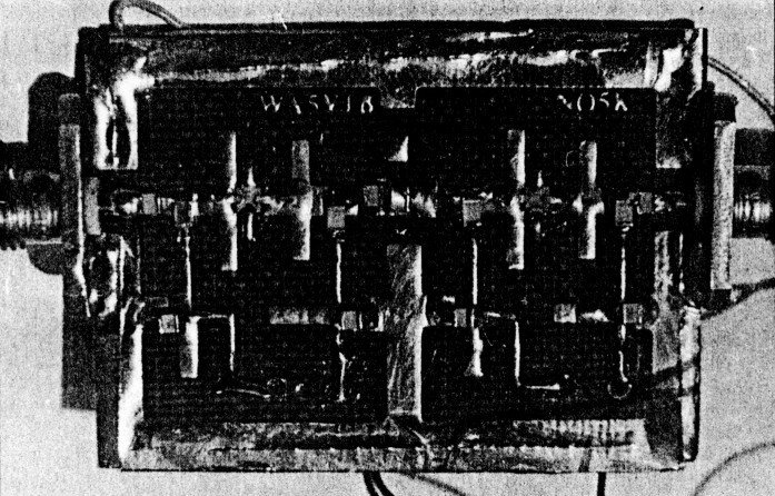
Photo B. N6IZW's 10 GHz pre-amp. GaAsFETs are mounted upside down, under the "W" and "N" in the callsigns. Coax connectors are SMA.
Next, mount the bias adjust circuitry, two 10k0 pots, on the back of the board. Pass the wiper of each pot through a small hole in the ground plane so that it contacts the bias feedpoint for FET#1 and #2. The opposite end of the adjustable potentiometer is grounded, and the high end is tied common to each other with a 10k ¼ Watt resistor in series with the bias supply. Place a small insulator under the pots to prevent the top negative supply point from possibly touching ground with any downward pressure on the pot. Tie the two drain lines common, on the back of the board.
When all components are mounted and the FET cutouts made, check the board carefully, then insert the GaAsFETs, one at a time, into the board. Use a grounded soldering station, and don't forget to ground yourself to the work piece. A wrist strap of high resistance, but sufficient to discharge any static from yourself, is available from many dealers. This is necessary to prevent damage to the sensitive FETs. If you take these precautions you should not have any trouble. Just work slowly and carefully, and keep all components grounded.
Final Check
In this last stage, pre-set the bias pots to maximum resistance, or maximum negative bias, to limit the FETs' drain current. Apply negative bias to both FETs, and while watching the first stage with a current meter (I used a 0 to 100 mA meter), adjust the associated bias pot to a drain current reading of 10 mA. (For the preliminary check, you might want to start with a positive DC voltage somewhat less than 4 volts.)
The first stage current of 10 mA is consistent with minimum noise figure according to the gain versus noise figure curves. Stage two is adjusted in the same way, except that you should adjust for a current reading of 20 mA. Higher current is not necessary, as the device is operating at optimum performance at this current level. For fine tuning anomalies, you may affix small pieces of copper to a toothpick and move around the traces of the PC board. We did not perform this step because we were satisfied with the gain we obtained. It was stable and very near optimum.
When you are satisfied with the operation, you can adjust the bias to minimum current and re-set the positive DC supply to 4.5 volts. Go through the same procedure to set current levels. Do not apply DC voltage, negative or positive, above 5 volts because 6 volts will destroy the device. Go slowly, don't rush, and think your operations through. You can measure three times, but you can cut only once.
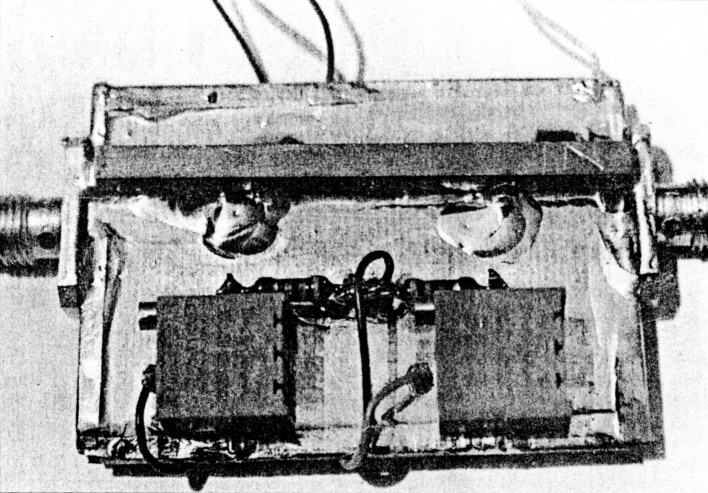
Photo C. Rear view of the 10 GHz preamp, showing the mounting arrangement of bias adjustment pots, and the brass bar which strengthens the soft Teflon PC board.
After the final checkout, put a short piece of scrap brass on the back of the PC board, over the soldered connection for the FET source case lead (see Photo C). Mount the brass to clear the other parts, and solder it between the two SMA flanges and the ground foil. This will reinforce the Teflon PC board. House the amplifier in a suitable, shielded container along with the power supply (see Photo D).
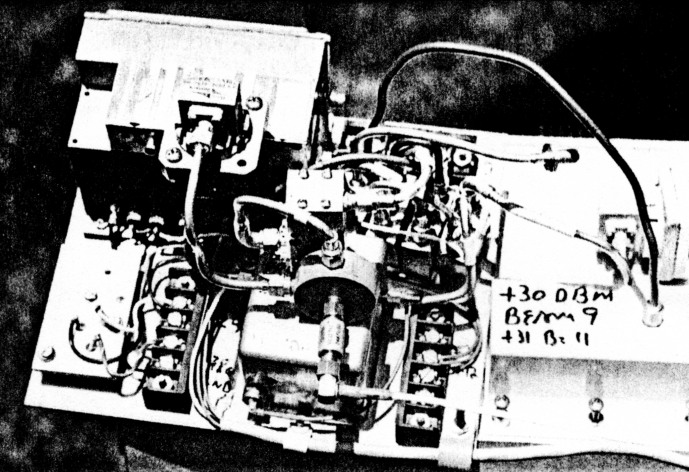
Photo D. 10 GHz SSB station WB6IGP uses 24 SMA connectors and 4 SMA SPDT 18 GHz relays. Preamp is inside the small bathtub-capacitor-looking shielded box. The large unit in the rear is the phase locked 10 GHz oscillator. See Figure 4 for block drawing.
Performance
From use, we know the amplifier is quite stable, with a good performance record. Most of the units we built varied due to different construction techniques, but they all gave close to 18 dB gain. The amplifier as both a receiving and transmit amplifier gave very good results. In transmit, the maximum output we obtained was +8 dBm as read on my HP-431 power meter. Kerry N6IZW and I feel that this is duc partially to the fact that the 100n drain resistor on the output stage limits the device. We plan to try changes by setting bias and replacing the 1000 resistor with a RFC. This will require further experimentation.
We made the relay switching scheme with four relays which happened to be the only microwave relays in our junk box. You can use other types, but check their loss, as the ones we used were less than 0.1 dB connection loss per contact. Cross isolation was excellent; loss from coupling from one operated side to the non-operated side was in excess of 50 dB. All interconnections were made with 0.141 coaxial hardline and SMA coaxial connectors.
The outline in Figure 4 shows our complete SSB system for 10 GHz. Other major parts of the system are the mixer and phase locked microwave oscillator. We obtained the latter from surplus. You can buy or build the the mixer. In another article, I will cover these items in detail.
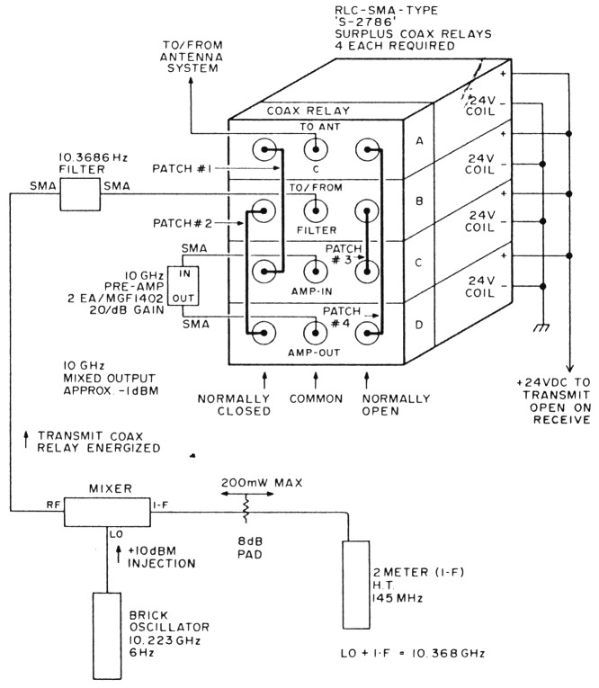
Figure 4. 10 GHz switching, for receive and transmit.
Conclusion
Construction of this amplifier will give you a very good preamplifier and versatile device for 10 GHz microwave band operation. We have also used this device on our spectrum analyzer to improve system sensitivity.
PC boards for the 10 GHz amplifier are available etched and ready for mounting parts, with the ground foil, for $10 each postpaid. A kit with the chip resistors and capacitors, SMA connectors (2), ground foil and PC board, is $20 postpaid. The switch mode power supply module is $5. Specify 5 volts or 12 volts input. I would be happy to answer any questions pertaining to microwave or related subjects.
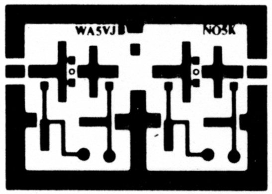
Figure 5. PCB foil diagram for 10 GHz preamp.
WB6IGP, C.L. Houghton.