NE5205 wideband RF amplifier
Inexpensive IC functions as small-signal amplifier to 600 MHz
Simple, inexpensive, wideband RF amplifiers are always much-needed items when experimenting in RF and constructing RF projects. Because each project has its various unique requirements that must be satisfied - minimum cost, low operating current, maximum bandwidth, and high output power, for example - one can never have too many different configurations from which to choose. But the ideal amplifier that satisfies all potential needs has yet to be invented; consequently, a different approach or new design is always welcome.
This brief article describes the construction of a relatively high-performance RF amplifier that uses a Signetics NE5205 wideband RF amplifier. The NE5205(1) is an integrated wideband RF amplifier that serves as an excellent general-purpose RF gain block for applications from a few Hertz to above 600 MHz. It provides a non-inverting 20-dB gain and, although not an LNA, its typical 6-dB noise figure (50-ohm input) is quite good and should be adequate for many RF projects.
The NE5205 is available in either a TO-46 metal package or an eight-pin small-outline (SO) package. Although samples were distributed in the conventional eight-pin mini DIP ("N" package), that package isn't shown in the NE5205 literature and doesn't appear to be available from distributor stock.
The SO package is a very inexpensive plastic unit with the same operating characteristics as the TO-46. A minor problem with the SO package, however, is size; it's about one-twentieth the volume of the more common eight-pin mini DIP. The leads, on 0.05-inch centers and bent at the ends in the form of small feet, are much too short to go through even a thin PC board. This is a surface-mount device (SMD) designed to be mounted on the trace side of the PC board or other substrate. The package is small, but it isn't difficult to handle; you will, however, have to be quite careful and you may have to buy a small tip for your soldering iron.
NE5205 features
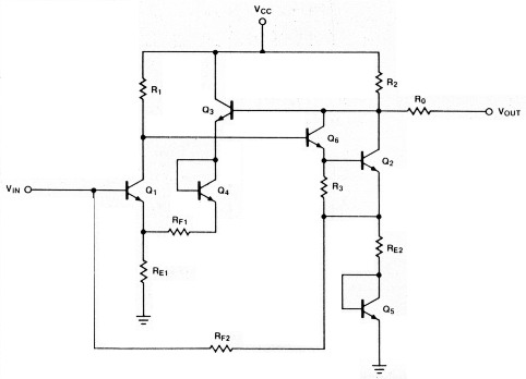
Fig. 1. NE5205 functional diagram.
The functional schematic for the NE5205, shown in fig. 1, is considerably more complex than typical integrated wideband RF amplifier gain blocks. The small die size, offering low propagation delays and low parasitic elements, in part give this component its good operational characteristics. A particularly useful feature is the use of several different feedback loops to stabilize the gain and operating point and provide good input and output impedance matching. While this is too lengthy a topic to be covered here, the NE5205 data sheet provides complete details.(1)
Don't try to build the circuit shown in fig. 1 from discrete components; such a construction might work to a few tens of megahertz, but in general its performance will be very poor at best. The success of this circuit design depends as much on the small die size and integrated construction as on the actual circuit configuration. In any event, it's much less expensive to use the NE5205 than to build a discrete version.
In a minimum basic circuit, the NE5205 needs only three external components: input and output coupling capacitors and a supply bypass capacitor. Adding a few inexpensive components, however, results in a more versatile amplifier with much better tolerance for the abuse of experimenting than a minimum parts-count amplifier would offer.
Amplifier circuit
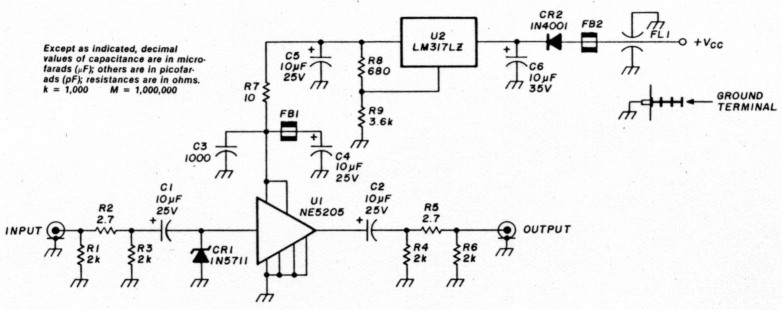
Fig. 2. Amplifier schematic diagram.
Figure 2 shows the schematic of the complete amplifier. The input diode, CR1, prevents reverse-bias damage to the input transistor of the NE5205. The input can generally tolerate short pulses of high forward bias since the input transistor is simply forward-biased. However, even short pulses of reverse (negative) input bias as low as a few volts will avalanche the input emitter-base junction, totally destroying the part or seriously degrading its noise performance. When CR1 is included, it will conduct with a reverse input drive of about 1.4 volt, limiting the input level to the NE5205 to a safe value. This diode is reverse-biased at about 1 volt by the input potential of the NE5205. Since the maximum usable input of the NE5205 is about 80 mV peak (-12 dBm), the 1 volt reverse bias of CR1 prevents its conduction with normal signals and helps reduce the diode capacitance to minimize loading of the input. CR1 is a Schottky diode with a faster response speed than the NE5205 and it has minimum capacitance. If you can't find the 1N5711 device specified for CR1, a 1N4148 or 1N914 will work reasonably well; the high-frequency cutoff may be reduced, however. CR1 may simply be omitted, but the finished amplifier will then be quite sensitive to input damage.
Resistors R1, R2, and R3 form a Pi pad to allow a little adjustment of the amplifier gain and input impedance. They also provide some additional input protection. Similarly, R4, R5, and R6 form an output pad for gain and output impedance adjustment. These two pads may be omitted for maximum gain, but I find that keeping about a 0.5-dB pad at each place provides better stability in general applications. The resistors should be a high-quality carbon composition type. Low-noise carbon film or metal film may be used if their high-frequency performance is adequate.
The coupling capacitors, C1 and C2, must be dipped tantalums to minimize the physical size and provide good high-frequency performance. Don't try to use aluminum electrolytics; if you do, you're likely to end up with an oscillator. Capacitors C3 and C4 are supply bypass capacitors. High-frequency bypassing is provided by C3, with C4 providing low-frequency bypassing. The ferrite bead, FB1, prevents the lead inductance of C4 from forming a parallel resonance with C3. Here the bead is acting like a very lossy inductance that totally destroys the Q of the C3/C4 resonant circuit. Without the bead, the parallel resonant network formed by C3 and the leads of C4 will cause. the effective power supply impedance to be high at the resonant frequency. This can cause an artifact in the frequency response and in some cases can cause instability (oscillation) due to coupling into the amplifier's internal circuitry through the power supply paths.
Resistor R7 helps to decouple high frequencies from the power supply pin, improving stability with cascaded amplifiers. With its associated components, regulator U2 protects the amplifier from over-voltage damage and stabilizes operation with unregulated supplies. It too may be omitted if a good 5- to 8-volt regulated supply is available, but it's generally more convenient to provide regulation as part of the basic amplifier design.
Diode CR2 protects the amplifer from the application of a reversed power supply voltage, probably one of the more common types of damage to experimental circuits. The power input filter FL1 prevents noise from coupling into the amplifier from the power supply leads. Bead FB2 on the filter lead provides a little additional filtering of the power supply input.
Choosing the correct PC board material
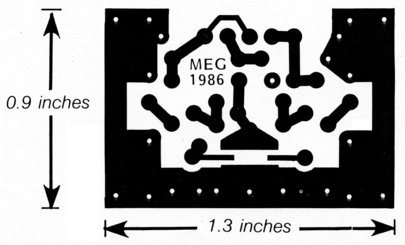
Fig. 3. 3:1 PC board artwork.
The 3:1 artwork for the amplifier is shown in fig. 3. This layout is tailored for installation in the enclosure discussed later; if you choose to use a different enclosure, you'll have to make some alterations to the mounting details, but don't change the basic circuitry unless you're experienced in RF PC board layout.
This board was designed for surface-mounting of all components even though only the SO-package NE5205 is a true surface-mount part. The PC board should be constructed of 1/32-inch, 2-ounce double-clad epoxy-glass material. Standard PC board doesn't make a good substrate for surface mounting because the pads will pull off easily, particularly during soldering. However, if you're careful, you can achieve quite adequate results. The only component holes necessary are those that tie to the ground plane. Since there are no component holes other than those grounded, there's no need to clear the ground plane from any of the component leads on the ground-plane side of the board. Only single-sided PC board construction is then required. A full ground plane is needed on the nontrace side, but no etching is required on the ground plane. This makes the board a bit easier to duplicate and consequently a little less expensive if you have it fabricated.
| Box | Pomona 3751 or similar (Newark Electronics No 34F1260/$18 50) |
| C1,C2 | Capacitor, 10 µF/25V dipped tantalum |
| C4,C5 | Sprague 1960 or similar |
| C3 | Capacitor, 1 nF CK05 or disc |
| C6 | Capacitor, 10 µF/35V dipped tantalum - Sprague 1960 or similar |
| CR1 | Schottky diode, 1N5711 (may substitute 1N914 or 1N4148 if the 1N5711 cannot be obtained) |
| CR2 | Rectifier diode, 1N4001 or equivalent |
| FB1,2 | Ferrite bead (Amidon FB-43-101 or equivalent) |
| FL1 | Filter, Erie 1250 003 or equivalent (Newark Electronics No 10F81451$3 13) |
| PCB | PC Board, per fig. 3 |
| R1,R3,R4,R6 | Resistor, 2 k, RCO7 carbon composition -- Allen Bradley or equivalent |
| R2,R5 | Resistor, 2.7 ohm, RCO7 carbon composition - Allen Bradley or equivalent |
| R7 | Resistor, 10 ohm, RCO7 carbon composition - Allen Bradley or equivalent |
| R8 | Resistor, 680 ohm, RCO7 |
| R9 | Resistor, 3.6 kilohm, RCO7 |
| U2 | Regulator, LM317LZ |
| Terminal | Ground Terminal, (Newark Electronics No 40F6026/$15.00/100 each) |
| U1 | RF amplifier, Signetics Electronics, NE52050 |
| Note: Jameco Electronics carries many of the above items and can supply most of the components (except the PC board) on an "After Receipt of Order" basis subject to their line-item and invoice minimums and distributor availability. | |
| A complete kit for this project is available from Radiokit, Box 411H, Greenville, New Hampshire 03048 Contact Radiokit for details. | |
Though it's easier to have the PC board fabricated, it's actually simple enough to make using a cut-andpeel technique. A small hobby knife can be used to cut the trace outline through the cladding on one side of a precut piece of double-clad PC board and a needle-nose or heavy tweezer used to peel the unwanted cladding from the board. While peeling, use a soldering iron to soften the adhesive and heat the cladding to be removed.
PC board assembly
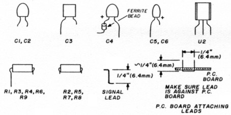
Fig. 4. Component lead forming details for surface mounting.
As I indicated earlier, the only component of this circuit designed to be surface mounted is the NE5205. The leads of the other components must therefore be bent to allow them to be mounted. Figure 4 shows how to bend the leads of the various components so that they can be mounted. Try to follow this lead dress carefully since lead length is reasonably critical because of the high maximum frequencies of operation of this amplifier.
Although assembly of the PC board is straightforward, some care is necessary because of the tight packing of the components. You'll need a soldering iron with a 1 /16th-inch tip to prevent solder from bridging between pads. Also, be very careful when mounting the five capacitors and the regulator. These are large components and their pads can be lifted very easily from the board when soldering. Both during and after mounting these components, take care not to bend them out of position; this would put considerable stress on the mounting pad and could cause the pad to become separated, particularly after soldering. When soldering to the ground plane, keep the solder buildup to a minimum, since there's very little space under the board in the enclosure.
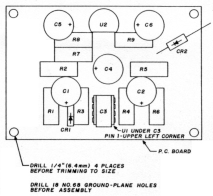
Fig. 5. Amplifier assembly drawing.
Figure 5 shows the assembly drawing of the PC board. Because it's probably the most difficult of the board components to mount - and because it will be partly covered by other components - mount the NE5205 first. The pin next to the "S" in Signetics is pin 1. The other components must be mounted in the order shown in table 1 because of the tight packing. After mounting the amplifier, mount C3 over the top of the amplifier with its leads straddling the NE5205. Then mount the remaining components in the order shown in table 1, noting the associated comments.
| 1. | NE5205 | Pin 1 is at the Signetics "S". |
| 2. | C3 | Above the NE5205, solder ground plane. |
| 3. | C4 | Observe polarity, remember the bead, solder ground plane. |
| 4. | R3 | Solder ground plane. |
| 5. | R4 | Solder ground plane. |
| 6. | CR1 | Observe polarity, solder ground plane. |
| 7. | Cl | Observe polarity. |
| 8. | C2 | Observe polarity. |
| 9. | R1 | Solder ground plane. |
| 10. | R6 | Solder ground plane. |
| 11. | R2 | |
| 12. | R5 | |
| 13. | R7 | |
| 14. | R8 | |
| 15. | R9 | Solder ground plane. |
| 16. | REG1 | Observe mounting orientation. |
| 17. | C5 | Observe polarity, solder ground plane. |
| 18. | C6 | Observe polarity, solder ground plane. |
| 19. | CR2 | Observe polarity, leave anode lead full length. |
When all the components have been mounted, bend four pieces of the resistor leads that were cut off during assembly into a "U" shape as shown in fig. 4 and insert them from the ground plane side into the four pairs of holes at the corners of the board and solder them to the ground-plane side of the board. Make sure that the portion of each of these leads that's on the ground-plane side of the board is flush against the ground plane. They will be used to ground the board and hold it in the box. Finally, solder pieces of cut-off resistor leads to the input and output pads (again, bend as shown in fig. 4).
After the board is assembled, clean it in isopropyl alcohol; a 91 percent solution - probably available from your local drug store - works best. Don't use denatured ethanol because the denaturing agent isn't known. I prefer alcohol to trichloroethane for PC board cleaning because it presents no known health hazard. But it is flammable, so take appropriate precautions.
Figure 6 shows the assembled PC board before mounting in the enclosure.
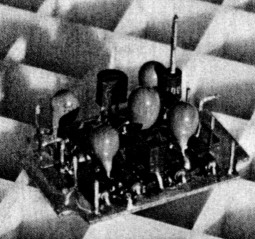
Fig 6. Assembled PC board.
Enclosure modifications
Enclosures for small RF projects are always a problem. The one I used for this amplifier was a small die-cast chassis box. This is a reasonably convenient enclosure; only two additional holes must be added for the power entry filter and the ground terminal. Figure 7 shows the details of the modifications to the box, the two RF connectors, and the mounting screws. A word of caution here: don't try to cut the screws with a pair of diagonal cutters; the screws are very hard and trying to cut them will damage the cutters. The tips of the screws will break off easily enough if you use a pair of pliers to hold the tip while you bend the screw body with your fingers. Carefully lay out the holes using a precision scale and scribe. Center-punch the hole positions before drilling to prevent the drill from "walking." Tap the holes carefully; the tap is very brittle and will break with only slight side pressure. While tapping, use plenty of oil on the tap to prevent binding. Every turn or two, back the tap out to clear the chips. This will also help prevent binding.
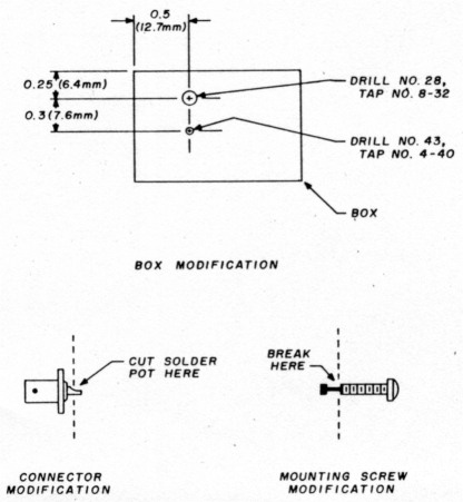
Fig 7. Box and connector modifications.
Final assembly
Now for the final task of putting it all together. With the Connectors and power filter removed from the box, place the assembled PC board into the box, component side up and oriented so that the regulator is at the side of the box with the power entry filter. Loosely mount the input and output connectors, using only the upper two holes and the two short screws provided with the enclosure. As you place the connectors on the enclosure, be sure that the input and output connecting leads fit inside the connector holes. Now insert the longer screws into the bottom holes and make sure that they're on the component side of the PC board and between the pairs of leads coming up from the ground plane. Tighten all the screws. Now, bend the pairs of leads near each lower screw over the screw, laying them in the relief at the end of the screw. Solder all four screws to the wires and PC board. You'll need a larger soldering iron than you used for the board assembly to get enough heat for a good solder joint. Make sure that the tip of each screw has a good solder bead to the PC board; the PC board is grounded to the box only at these four places. Try to avoid getting solder in the screw threads so that the screws can be removed if you have to'remove the board for repair later on. Solder the input and output leads to the connectors. Mount the ground terminal and power entry filter. If you cannot find a ground terminal, use a 4-40 brass screw about 1/2 inch long. Place a nut on the screw and screw it into the box until it's just penetrating the inside by a thread or two. Then tighten the nut down against the box to lock the screw in place. Place the bead, FB2, over the filter lead and attach the lead of CR2 to the power filter. Hold the body of CR2 with needle-nose pliers while bending its lead to prevent stressing its PC board mounting pad. Trim off the excess filter and diode lead.
Do a final cleaning by filling the assembled box with alcohol and letting it sit for a few minutes. Place your hand over the open top and shake the unit to stir the alcohol. Pour it out. Rinse with a little more alcohol and pour that out. Let the alcohol evaporate for a few minutes and then fasten the cover.
Figure 8A shows the completed amplifier assembly with the cover removed; fig. 8B shows the completed assembly.
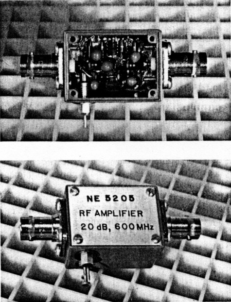
Fig. 8. Completed amplifier assembly, A) Internal view, B) with cover on.
Performance
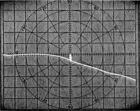
Fig. 9 Amplifier frequency response.
Now for the proof test: how well does the amplifier work? If you followed the assembly instructions carefully, it should work rather well. Figure 9 shows the frequency response of the unit that I built. The gain was 20 dB with a lower 3-dB point of 270 Hz and an upper of 608 MHz with usable gain to beyond 1.2 GHz. The bandpass flatness in the bandpass was better than ± 0.5 dB. The wideband noise figure was about 5 dB - not an LNA but certainly quite good. The output power at the 1-dB compression point at 100 MHz was +6.7 dBm, and the compression was reasonably constant with frequency up to about 600 MHz (the upper 3-dB cutoff frequency). The total supply current was about 35 mA and the minimum operating potential about 10 V. Figure 10 shows the S-parameters S11 and S22 for the completed unit. These parameters are a ratio of the forward and reflected power at a given port. In fig. 10 S11 is below about -20 dB up to about 500 MHz. The S11 parameter in this measurement was made at the input port. The - 20 dB value shows that the power reflected back from the input is 20 dB below the power incident at the input port. That implies that the input impedance is reasonably close to the 50-ohm impedance of the test system; no power is reflected from a perfectly matched load. With a 20-dB return loss, the input impedance is within about 0.5 ohm of the characteristic 50-ohm impedance. S22 is the output port measurement. Up to about 500 MHz the reflected power from the output port is more than about 20 dB below the incident power at the output port. In this S22 measurement, power is actually applied to the output and the reflected power measured. So the output impedance is also reasonably close to 50 ohms (within about 0.5 ohm).
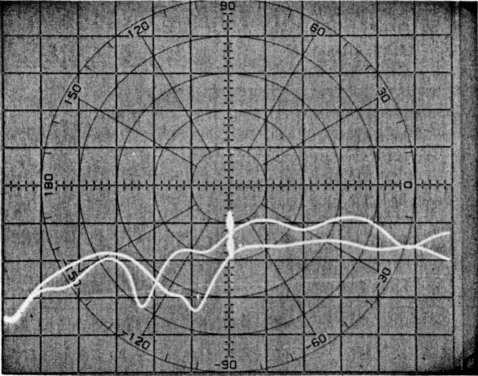
Fig. 10. Input (S11) and output (S22) S-parameters.
Conclusion
This amplifier, if carefully constructed, provides very good performance for general RF experiments and RF projects where a relatively low cost, stable, low-noise, wide-bandwidth gain block is needed. The characteristics of the NE5205 make it a good choice for this application and the recommended circuit design assures both RF and DC stability as well as protection from typical experimental abuse. The recommended packaging provides good RF shielding and isolation, assuring stable, noise-free operation in most common RF environments. It is also relatively easy to construct. This amplifier should be a very useful addition to your collection of general RF amplfier designs.
References
- Signetics NE5205 data sheet, January, 1985, Signetics Corporation, 811 East Arques Avenue, P.O. Box 3409, Sunnyvale, California 94088-3409.
- Newark Electronics, 277 Fairfield Road, Fairfield, New Jersey 07006.
- Amidon Associates, Incorporated, 12033 Otsego Street, North Hollywood, California 91607.
Michael E. Gruchalla.