The ubiquitous diode 2
Last month's column discussed the electrical and mechanical properties of solid-state diodes, with emphasis on the most important parameters.(1)
This month we'll focus on specific applications using solid-state diodes, emphasizing circuitry and how to select the right diode for each particular application. Some of the applications we'll cover are rectifiers/detectors, regulators, mixers, switches, limiters, tuning elements, multipliers, oscillators, and optical devices.
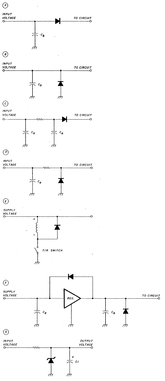
Fig. 1 - Typical solid-state reverse power supply protection circuits. In all circuits CB is a 0.01 to 0.1 µF ceramic disc capacitor as recommended and described in the text. (See text for recommended protection diode types.) (A) is most common where the extra voltage drop is not important; (B) is used where no supply voltage drop is permitted. (C) is recommended for extra protection; ID) is used for extra shunt protection. (E) uses a reverse polarized diode across all relay coils to reduce inductive spike generation and (F) use a three-terminal regulator with two additional protection diodes to prevent regulator burnout. In (G) zener diodes should always be bypassed to decrease low-frequency noise. A 10µF or greater solid tantalum capacitor is recommended.
Simple diode applications
VHF/UHFers seldom give adequate notice to the use and abuse of low-frequency diodes. They forget that the diodes in a power supply or dc protection scheme are often just as important to system reliability and performance as the VHF/UHF diodes in rf circuits.
For instance, it makes little sense to use vacuum tube rectifiers, which generate rf noise and have a very short lifetime when compared with properly installed solid-state rectifiers. Furthermore, solid-state diodes are instantly ready to operate; no warm-up time is required. This is particularly important in bias supplies for high-power vacuum tube amplifiers where you need to have proper bias applied before energizing the high voltage.
While on the subject of high-voltage rectifiers, the economy and reliability of a single packaged unit is recommended.* Using strings of diodes, resistors, and capacitors for high-voltage rectifiers is an open invitation to failure and is really no longer cost-effective. I can attest to this because I once used such arrangements before complete packaged units were available.
Before leaving dc applications, don't forget the lowly "idiot diode." If you leave it out you are an idiot.(2) Idiot diodes are used to prevent connecting the dc power with reverse polarity to a solid-state circuit. Few solid-state devices will survive such an accident.
Some typical reverse protection circuits are shown in fig. 1. The circuit in fig. 1A is by far the most common,(2) but will induce an additional voltage drop of approximately 0.7 volts, which may be unacceptable, especially in power amplifier applications.(3) The circuit illustrated in fig. 1B eliminates the voltage drop problem. However, using a small signal type diode in this circuit may still cause burnout if the circuit is improperly powered. Forward current in this circuit is limited only by the supply and the diode resistance. Therefore, its protection effectiveness decreases if the power supply currentcapability is higher than the diode can handle.
The circuits illustrated in figs. 1C and 1D are recommended to prevent idiot diode burnout. They can be used with small signal diodes if the voltage drop across the series resistor is acceptable. This is often acceptable, especially when using low-voltage devices such as GaAsFETs.(4) Typically 50 to 100 ohms of series resistance is sufficient.
However, some diodes, especially high-speed types or those designed for use in computers, are fast enough to respond to hf signals. Any rf coupled into the power supply line, especially from a local hf transmitter, can be rectified by the idiot diode and increase the circuit voltage above that from the supply alone.(5)(6) Therefore a large (0.01 to 0.1 µF typical) bypass capacitor at the power supply input terminals is recommended to bypass any rf before it reaches the idiot diode.
Low-frequency diodes are also used to bypass relay coils (fig. 1E). This diode, which Amateurs often leave out, is recommended because the transient induced by the de-energizing of a simple T/R relay can cause large voltage spikes to appear on power supply lines.
Therefore, never connect solid-state circuits, especially those used for lownoise amp/ifiers, to a power supply that is also used to supply a relay. This is an open invitation to disaster because the voltage spikes generated by opening a relay coil can destroy other circuits connected to the same power supply.(6)
The zener is another diode popular with VHF/UHFers. Actually, this type of diode is working in a normally forbidden mode - in the reverse biased or avalanche region. By careful manufacturing control, the breakdown voltage of the zener is predetermined along with the series resistance of the diode. The heat dissipation in the junction must also be removed so that thermal runaway or junction burnout does not occur.
A zener diode makes a reasonable voltage regulator or limiter with a stable breakdown voltage within a specified current range. Zeners should be used with care, however, especially as voltage regulators for oscillators, because they generate broadband low-frequency noise in the avalanche mode.
If you use a zener in an oscillator circuit, be sure to provide adequate low-frequency bypassing such as a high-value (10 to 100 µF) bypass capacitor (fig. 1G). Personally, I prefer to use the newer three-terminal voltage regulators rather than zeners because they are quieter and usually have a wider regulation range versus output current than most zeners.(4)
Finally, it has been shown that under certain operational conditions a three-terminal voltage regulator can be damaged. The addition of two extra diodes around the regulator is suggested (fig. 1F).(6)
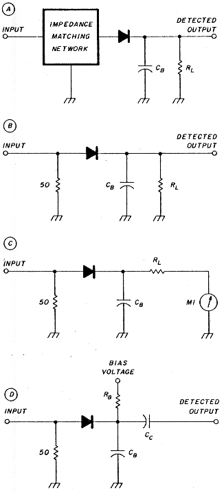
Fig. 2 - Typical diode detector circuits. (See text for recommended diode types.) In all cases CB is an rf bypass capacitor. A feedthrough type 0.001 µF capacitor is recommended. R1 is the video load (10k ohms typical).
(A) is recommended in narrowband applications where maximum detector sensitivity is desired. (B) shows a simple broadband detector. The 50-ohm resistor should have good rf characteristics. (C) illustrates a method for using the circuit shown in fig. 2B for power detection with a meter; (D) shows a method for increasing the sensitivity of an HCD by applying an external bias voltage. CC is a dc blocking capacitor and Re is the do biasing current resistor as explained in the text.
RF detectors
One of the first major VHF-andabove applications of solid-state diodes was as rf detectors. This application, which dates back to the "good old a-m days," is still quite prevalent, especially as the detector in police radar! Rf detector diodes are also widely used today in VSWR and rf power meter applications.
Good rf detector diodes can be quite sensitive. The lowly point contact diode can detect rf below -60 dBm (200 microvolts rms in a 50-ohm system).(1) However, this will probably require some additional amplification at the output of the detector. At somewhat higher rf input levels (greater than -10 dBm or 70 millivolts), this same diode can directly drive a microammeter for power measurements.
Some typical rf detector circuits are shown in fig. 2. Figure 2A shows an optimized detector with an input matching network. Most detector diodes have a high input impedance. Therefore, the circuit in fig. 2A may exhibit narrow bandwidth.
If wide bandwidth is desired, the simple circuit in fig. 2B is usually used.(7). It has lower sensitivity than a matched detector, but this is easily traded off for the wider bandwidth capabilities. If a meter is added in series with the detector output load (fig. 2C), a detector can be used directly as a power meter over a wide frequency range.
Before designing a detector, it is important to compare the various typesof diodes that were mentioned in reference 1. The most common detector types are the point contact, the silicon junction, and the Schottky or hot carrier diode (HCD).
The point contact diode, the first sensitive solid-state detector diode, was followed by the much less sensitive junction diode in the late 1950s. First introduced in the 1960s, the HCD is 20 to 30 dB less sensitive than a typical point contact diode. However, the HCD is still more sensitive than the typical silicon junction diodes because it has a lower barrier voltage.(1)
In the mid-1970s, the zero-bias.HCD was developed. It has a very low barrier voltage, making it an ideal small signal detector. Typical input-versusoutput voltages for the types of detector diodes just discussed are illustrated in fig. 3.
Note in fig. 3 that below about - 20 dBm (22 millivolts) most detector diodes have what is called a "square law" region where the output or detected voltage doubles each time the input power is doubled. However, above -10 dBm (70 millivolts) most detector diodes have a detected outputvoltage that is a linear function of the input power level. In between these rf levels is a very nonlinear region where compression takes place.
Nowadays, the low- to medium-barrier voltage HCD is usually preferred for detector applications. However, to make it competitive in dynamic range and sensitivity with point contact diodes, the barrier voltage must be overcome. This can be accomplished easily with a small amount (5 to 20 microamperes) of forward bias current applied as shown in fig. 2D.
Properly biased, the HCD offers greater forward conductivity (more output voltage for a given input power level), almost zero recovery time, and low cost. Furthermore, HCDs usually have a better impedance match than other types of diodes. They have vastly lower microphonics than other types of detector diodes. HCDs also have less flicker or 1/f noise, a phenomenon in which the noise figure of a device increases with decreasing frequency, especially below 10 kHz. Point contact diodes are very noisy and therefore unsuitable for radar applications, in which the information returned is in the very low or subaudible frequency range.
Some precautions must be observed with HCDs. They normally have a low peak reverse breakdown voltage as discussed in reference 1. When a higher reverse breakdown voltage (15 to 75 volts) is required, a "guard ring" structure must be added internally to the diode chip by the manufacturer. However, this increases junction capacitance and thus decreases the upper frequency limits of operation.(1)
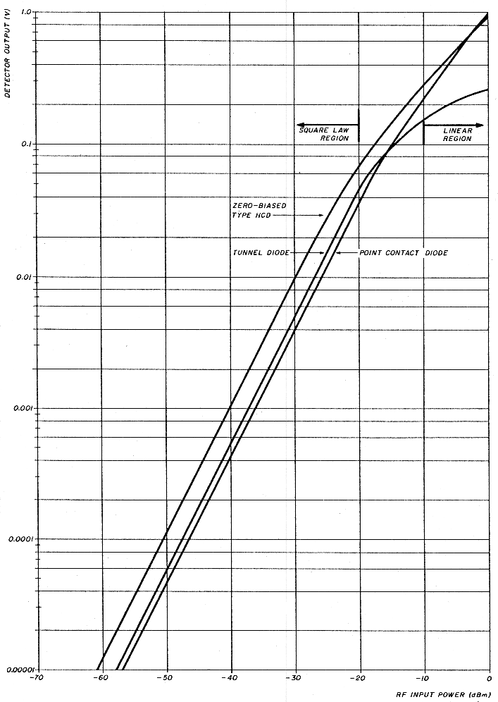
Fig. 3 - Typical output voltages for different types of detector diodes versus rf input power level into a 10-k load resistor using the circuit shown in fig. 2A.
Tunnel diodes
One diode that I didn't mention previously, but is often used for rf detectors, is the tunnel diode, sometimes referred to a5 the Esaki diode after its inventor, Dr. Leo Esaki, who discovered the effect in 1959. It's also referred to as a "back" diode because its main current flow is in the back biased rather than the forward biased direction. It has high sensitivity at very low rf input levels, utilizing the quantum mechanical tunneling effect.
Tunnel diodes may be manufactured using different semiconductor materials such as germanium, silicon, or gallium arsenide, depending on the frequency range desired. The main drawbacks of tunnel diodes are difficulty of manufacture (because they require a highly doped alloy junction), a lower burnout level, and a narrow dynamic range, typically only 40 dB, as opposed to 60 or more dB for a good point contact or zero bias hot carrier type diode (fig. 3).
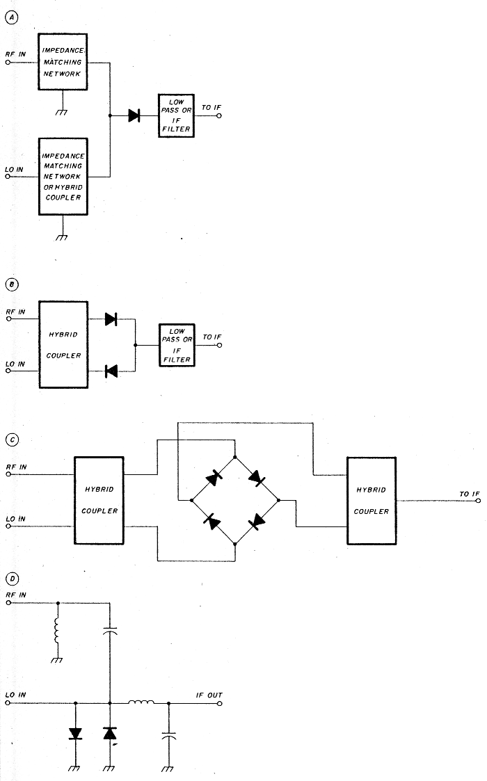
Fig. 4 - Some typical mixer circuits: (A) shows a single-ended mixer (see text for filtering explanation). (B) is a balanced mixer using a hybrid coupler to isolate the rf and LO. IC) shows a double-balanced mixer using two hybrids; (D) illustrates a subharmonic mixer using a pair of antiparallel connected mixer diodes.
Mixers
Frequency conversion or mixing is the process which converts a signal at a low power level from one frequency to another by combining it with a higher level signal such as the local oscillator (LO) in a nonlinear device such as a mixer diode. In theory, this mixer diode generates an infinite number of sum and difference frequencies called the i-f or intermediate frequency as well as harmonics of the input and local oscillator frequency.
In practice, only a small portion of the available rf signal power is converted to the i-f. This ratio of signal level to i-f power is referred to as conversion /oss. This loss is primarily a function of the local oscillator level (or rf bias), the diode junction, the diode's parasitics, and the mismatch at the rf and i-f frequencies. At higher frequencies, the junction capacitance becomes a primary limitation because it tends to bypass the junction resistance.(1)
Figure 4A shows this mixing process schematically in a circuit which is usually referred to as a single-ended mixer. If the mixer is a downconverter, the typical receiver type, both the local oscillator and rf matching networks should be high-pass filters so that the i-f isn't shunted to the input. Conversely, the i-f port should be a low-pass filter type of matching network so that only the i-f is present at the output. For upconversion, the filters/ matching networks are reversed accordingly.(9)
Most good detector diodes work well as mixers in a single-ended configuration. Point contact diodes were used for many years before the HCDwas available. The HCD is preferred since it has lower parasitics, lower series resistance, higher conversion efficiency, and low storage time and the ability to switch from the on to the off state in almost zero time.
The single-ended mixer has many disadvantages. The matching networks all have loss and restrict bandwidth. As the i-f, rf, and LO frequencies converge, filtering becomes more complicated and the conversion loss increases accordingly. It is also difficult to adequately filter out all the frequencies causing increased conversion loss.
Some of the impedance matching disadvantages of the single-ended mixer can be overcome by using a 90- or 180-degree hybrid coupler in a balanced mixer such as shown in fig. 4B. The hybrid transformer isolates the LO and rf from each other. However, the i-f matching/filtering is still a problem and twice as much LO power is required. The double-balanced mixer or DBM solves most of these problemsand is essentially two single-ended balanced mixers connected in parallel and 180 degrees out of phase (fig. 4C).
Actually, the DBM is really acting as a switch rather than a nonlinear junction. If the diodes are all similar (matched) and the transformers are well balanced, the rf, LO, and i-f ports will be well isolated from each other. Furthermore, there is suppression of the even-order harmonics, which significantly reduces intermodulation products. Finally, since the LO power is four times that required for a single-ended mixer, and less rf is across each diode, theintermodulation distortion is greatly improved.
Low series resistance and almost zero charge storage time make the HCD the ideal diode for a switching type of mixer. Furthermore, diode manufacturing technology now permits HCDs to be manufactured as either beam lead, monolithic pairs, or monolithic quads of diodes all closely matched on a single miniature substrate with a minimum of parasitics. The DBM works well as a mixer and is very simple to implement in up- or downconverters. Further use and applications of the DBM are discussed in references 8 through 10.
A newer type of mixer is the subharmonic configuration," which uses two diodes in antiparallel connection (fig. 4D). The chief advantage of this type of mixer is that the LO operates at half the normal frequency, so fewer LO multipliers are needed; this represents a significant breakthrough on millimeter-wave frequencies.
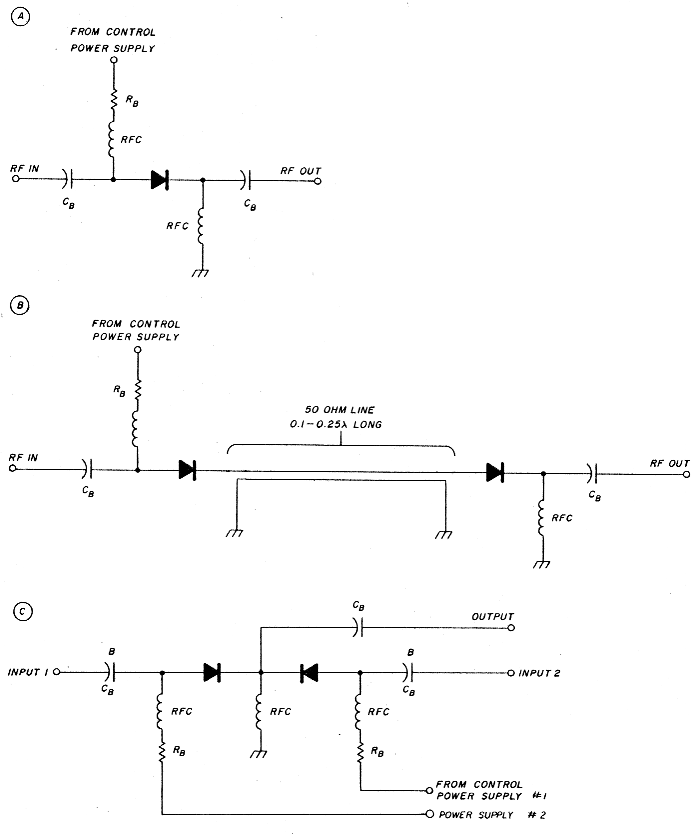
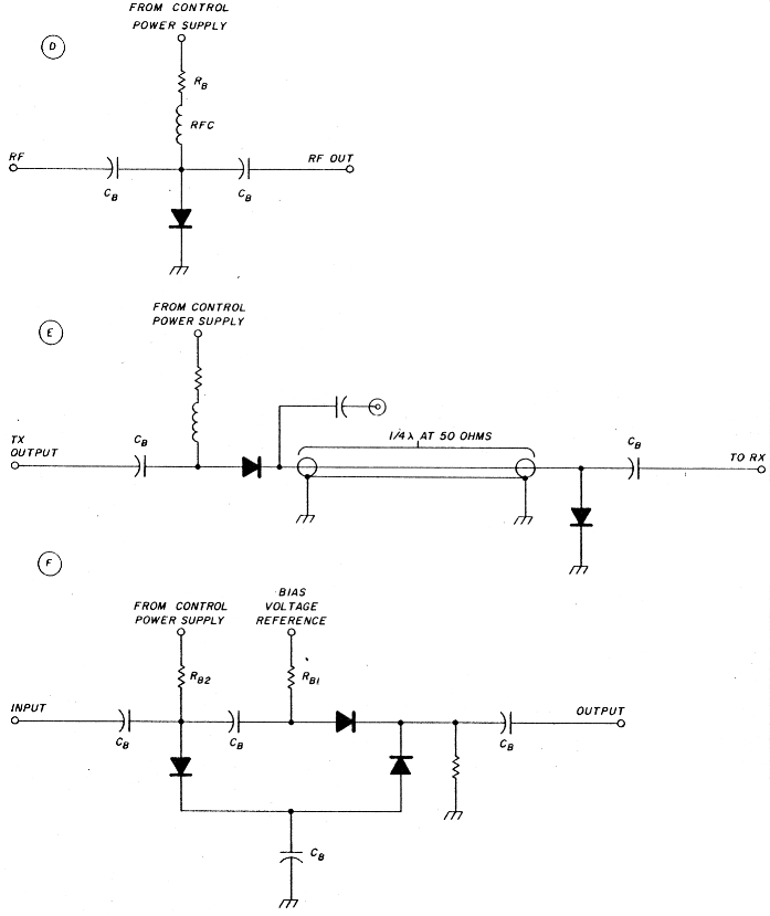
Fig. 5 - Typical rf PIN switch circuits. CB is a blocking or rf bypass capacitor. (A) is a simple series switch; (B) shows cascaded "switches" for additional isolation (see text for explanation of transmission line length). (C) shows a two-pole switch; (D) a shunt switch; (E) a typical T/R switch; and (F), typical PI type of variable attenuator.
Switches
Diodes can make excellent switches because they usually require only low forward current and can be remotely situated from the power supply. Therefore they can be located close to the circuitry to be switched.
Because of its high speed and fast recovery time, the HCD can be a good switch. However, its series resistancemay be too high if low insertion loss is important. The HCD is also a good rectifier, as discussed earlier. Therefore HCDs can introduce some loss and intermodulation distortion, especially if the rf level across the diode is sufficient.
The PIN (positive-intrinsic-negative), a three-layer diode, was invented accidently in 1956 and is now the most widely used solid-state switch. A PIN diode is actually no more than a lousy rectifier. The longer its "lifetime" (the inability to rectify in the presence of rf), the less likely it will be to cause inter-modulation. Diodes with at feast a 1-to 2-microsecond lifetime can be used in the hf region. Shorter lifetimes are fine at VHF and above.
When reverse biased, the middle or intrinsic layer of a PIN diode has extremely high resistance, with a small shunt capacitance. When a PIN diode is forward biased, it takes a finite time to switch to the "on" state. When forward biased, it acts like a current-controlled resistor: the greater the forward dc current, the lower the resistance.
PIN diodes are often used to switch rf because series resistances of less than 1.0 ohm are available. An example of a simple PIN diode switching circuit with low insertion loss is shown in fig. 5A. Low-capacitance PIN diodes will yield the highest isolation in the de-energized state, especially at the higher frequencies.
For very high isolation, two switch sections can be cascaded with a transmission line between the diodes (fig. 5B). For maximum isolation, the length of the interconnecting transmission line should be between 0.1 to 0.25 wavelengths, as explained in reference 5.
A typical two-pole PIN switch circuit is shown in fig. 5C. Commercially packaged two-pole, high-power switches suitable for switching over 100 watts through 1000 MHz (such as the M/A-Corn MA8334 series) are now available. These high-power PIN diode pairs are available in a threaded stripline package for minimum VSWR and maximum heat dissipation.
So far, the circuits illustrated use the series configuration. PIN diodes can also be used in shunt as illustrated in fig. 5D. An example of a shunt and series switch combination used as a T/R switch to provide extra receiver protection is shown in fig. 5E. Again, note the diode separation as described in reference 5.
Often used as variable attenuators, PIN diodes can have a very linear attenuation characteristic. The circuit shown in fig. 5A can be used as a variable attenuator by making R1 and/or the power supply voltage adjustable. More complicated circuits such as "L," "T," and "PI" types with up to three PIN diodes are also in wide use. An example of a typical "Pl"-type variable attenuator circuit appears in fig. 5F.
Most PIN diodes specified for variable attenuator applications have a graded resistance versus control current, so you may need a wide range of current - 0.1 to 50 mA, typically, but this is a function of the type of PIN diode used. PIN diodes used for switching often require only a nominal fixed current. Remember that all PIN diodes used in the hf region must have longer charge carrier lifetimes to prevent intermodulation distortion.
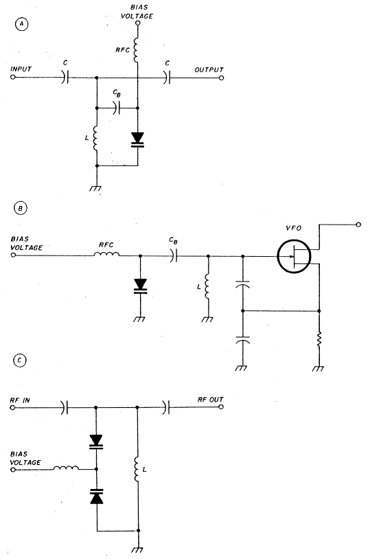
Fig. 6 - Typical varactor circuits. Component values depend on frequency and application. (A) shows a simple filter tuning circuit; (B), a varactor tuning a VFO; and ICI, series varactors to improve signal handling capabilities of a filter or oscillator.
Tuning diodes
Varactors (sometimes called "varicaps" or tuning diodes) were first developed in 1958. Basically a voltage-dependent capacitor, as described in reference 1, it is always operated with reverse bias across the diode.
Most varactor diodes are used to vary the frequency of a filter or oscillator. Varactors are especially common in places where only a small capacitance change is required, such as in a BFO or RIT control. A typical remotely tuneable filter using a varactor diode is shown in fig. 6A; fig. 6B shows a VFO circuit application. High-Q, low-capacitance varactors are still used in parametric amplifiers, where the diode is pumped with an external oscillator (usually called the pump) to act as a low-noise, high-gain amplifier. Note that the electronic symbol for a varactor diode is different from a standard diode with a sort of capacitor symbol tacked on to the cathode terminal.
In some applications there is sufficient rf voltage across a varactor diode to cause forward biasing, rectification, and distortion - a very undesirable situation. This phenomenon can be significantly improved or eliminated by using back-to-back varactors as illustrated in fig. 6C. However, the capacitance of each diode must then be doubled because they are now in series.
Because so many types of varactor diodes are available, many different capacitance-versus-voltage, or "CV" characteristics, may be obtained. Some examples of CV curves were provided in fig. 5 of reference 1, so they will not be repeated here. Examine the CV characteristics desired for your application to see whether abrupt or hyperabrupt tuning characteristics are required.
Finally, when selecting a varactor diode, always check the supplier's data sheet carefully for the recommended frequency range, Q, nominal capacitance at -4 volts (the standard reference voltage), and the available tuning range. Always operate a varactor so that it doesn't become-forward biased. If that is a problem, use a diode with twice the capacitance and the circuit recommended in fig. 6C as just described.
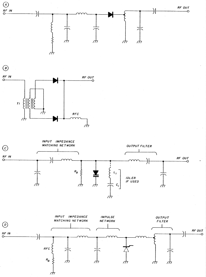
Fig. 7. Typical multiplier circuits. Component values depend on frequency and application (see text). (A) is a simple diode multiplier. (B) shows a balanced doubler using HCDs, and (C), a varactor multiplier circuit. The idler circuit is used for tripler applications. R8 is typically 50 td 100 k. (D) is a typical SRD multiplier. R8 is typically 200 to 500 ohms.
Multipliers
Diodes play a very important function as frequency multipliers. There are at least three types of diode multipliers in common use: varactor, resistive, and "step."
I'm sure that most readers have seen multiplier circuits where a diode is driven with a moderate amount of rf, typically 1 to 10 milliwatts, in order to generate harmonics. A typical circuit example is shown in fig. 7A.
In this particular application, the available harmonic power is primarily a function of the diode's nonlinear capacitance-versus-voltage characteristic and the stored charge in the diode, as mentioned earlier. In both regards, the point contact or typicalsilicon junction diodes (even 1N914s have worked!) are preferred because they generally have a greater nonlinear capacitance change near zero bias and are more likely to take longer to "dump" the stored charge, which is a desired characteristic of a good multiplier.
The HCD would be a less efficient multiplier in the above configuration because it falls into the resistive multiplier class. It has very little capacitance-versus-voltage change (see fig. 5 in reference 1) and is known for its quick switching response or ability to dump the stored charge almost instantly, as mentioned earlier.
However, if you operate an HCD in a balanced doubler configuration (analogous to a typical 60-Hz full wave power supply rectifier) similar to the frequency doubler circuit provided in reference 12, high efficiency can be obtained. Using HCDs in the circuit shown in fig. 7B yields good doubler efficiency results (only 6 to 12 dB conversion loss.) Furthermore, the fundamental and third harmonics are typically rejected by 20 to 30 dB. Hence less output filtering is required.
Although balanced HCD doublers have moderate conversion loss, they are very stable and have low noise. Sometimes they're easier to work withthan transistor doublers. With the availability of silicon MMICs (microwave monolithic integrated circuits), the conversion loss of a balanced HCD or the single-ended diode multiplier as described above can be inexpensively brought back to unity or greater gain as described in reference 12. I've been using this technique for many years with great success, and was doing so even before MMICs were available.
Moderate power (5 to 50 watt) varactors have been used for many years as doublers and tripiers up through 23 cm (1296 MHz). Diodes such as the surplus Microwave Associates MA 4060 low-cost, threaded-package, high-power varactor are in widespread use.(13) Even small signal varactors such as those discussed earlier for tuning oscillators and filters will work well at low input power levels (10 to 1000 milliwatts).
A typical varactor diode multiplier circuit (fig. 7C) consists of an input matching network, a varactor diode with its associated bias resistor, RB and the output filter network. Although their efficiency decreases when varactors are used as tripiers, it can be enhanced considerably by adding an idler circuit. This circuit consists of a high-Q series circuit tuned to the second harmonic of the input frequency (fig. 7C).
SRD multipliers
The SRD (step recovery or "snap" diode) is the "king" of multiplier diodes, especially when high efficiency and higher order multiplication (greater than 3 times) is required.(14) SRDs have a structure very similar to that of a PIN diode.
The capacitance of an SRD can usually be assumed to be independent of minor voltage changes and has a CV characteristic similar to that of an HCD'. When the rf input voltage goes positive, the diode turns on and stores a charge in the intrinsic region. When the applied voltage goes negative, it takes a finite time for the stored charge to decrease (the "snap" time), at which time the diode will abruptly turn off. During this transition period, the SRD conducts current for a very short period of time as if in a short circuit. This rf current is very rich in harmonics.
A typical SRD circuit is illustrated in fig. 7D. Note that the SRD has a different electronic symbol than other diodes. At first glance the circuit closely resembles that of the varactor multiplier (fig. 7C). However, there are a few subtleties. The input circuit has an extra section or "impulse" network, as illustrated. The bias circuit is slightly different. In the case of the SRD multiplier, a very low value bias resistor is used (typically 200 to 500 ohms, versus 50 to 100 kilohms for the varactor multiplier).
Another version of the SRD is the BIMODETM or A modeTM diode, which is enhanced for high power and high efficiency operation as a doubler or tripler. For best efficiency as a tripler, this type of diode requires an idler circuit similar to the one in a varactor multiplier (fig. 7C).
SRD multipliers can have conversion losses as low as a few dB - hence their popularity as multipliers. SRDs are usually capable of operation at up to 5 to 10 watts of power. If higher power (up to 50 watts) is required, SRDs are available in stacked or multichip packages.
SRDs are often used as impulse or "comb" spectrum generators for generating harmonics over a large frequency spectrum, as described in reference 14. Further information on designing SRD multipliers or combgenerators is beyond the scope of this month's column, but interested persons are encouraged to seek out copies of references 15 and 16.
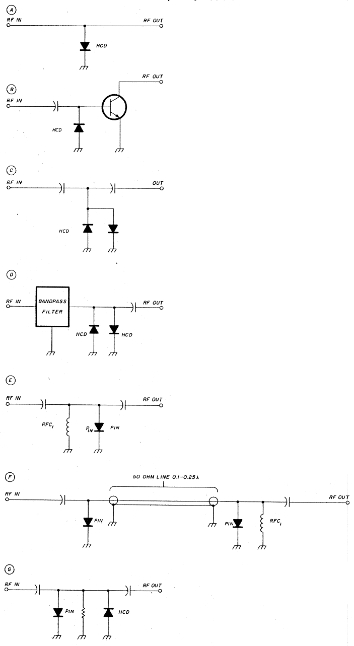
Fig. 8. Typical limiter circuits: (A) shows a shunt diode; (B), bipolar transistor protection; and (C), a back-to-back limiter. (D) illustrates the preferred configuration for a limiter; (E) shows a typical single-ended PIN diode limiter; and (F) illustrates the use of two different PIN diode types for high power applications. (G) Adding a shunt HCD to a PIN diode limiter will improve turn-on speed and lower rf limit level.
Limiters
It's often wise to place a circuit ahead of the input to your receiver to provide protection from stray rf, T/R relay leakage, or static.(6) Such a circuit is often referred to as a limiter. The simplest limiter is a diode, typically an HCD, connected to ground across the input line to a receiver (fig. 8A) or from the base to emitter of a bipolar transistor (fig. 8B).(2)
This type-of circuit is poor at best because it conducts only on one side of the input signal. Back-to-back diodes (fig. 8C) are better. However, neither configuration provides any protection from stray out-of-band rf. As a result, if moderate rf power is present on your transmission line, harmonics that will overload or degrade receiver performance may be generated by the limiter. Furthermore, HCDs can handle only low power (less than 1.0 watt); because they have a very low barrier voltage, 0.3 volts, they are easy to overload.(1)
Placing a bandpass filter ahead of a limiter (fig. 8D) helps. (This was recommended in references 2 and 6.) A further limiter improvement would be to include the diode within the filter so that the capacitance of the diode could be tuned out. If the HCD barrier voltage is too low, diodes can be hooked in series until a suitable "turn-on" voltage is obtained. However, the HCD is a poor choice for a limiter diode because it's really a rectifier and doesn't have a very low impedance, even when turned on hard.
On the other hand, a PIN diode with a very thin I (intrinsic layer), typically 2-10 microns thick, makes an excellent rf limiter. PIN limiter diodes act like a power -dependent variable resistor with very low turn-on resistance through the mechanisms of charge injection and storage similar to rectification. Because of the long carrier lifetime of the PIN diode, only one diode is needed, since it stays on for a longer period than the rf cycle.
A single such PIN limiter diode can be substituted for an HCD (fig. 8E). If the I region is very thin, the diode can respond in nanoseconds. PIN limiter types of diodes have very low resistance and don't rectify the same as HCDs, as described earlier.
Thicker I region diodes with up to 50nanosecond turn-on times are used for higher power operation. Power handling up to/in excess of 10 kilowatts for 1 microsecond duration is now possible! A thin and thick PIN limiter diode can be cascaded for additional protection (fig. 8F). Again, separate the diodes by 0.1 to 0.25 wavelengths, as discussed in reference 6. The inclusion of an HCD in the circuit shown in fig. 8G will help speed up turn-on time of a thick PIN limiter, especially at low power levels, for further low-power protection.
Noise diodes
So far I haven't mentioned the noise diode, a special type that works in the avalanche mode similar to the operation of a zener diode. These diodes aren't always easy to construct and therefore are usually more expensive than conventional ones.
Noise diodes are particularly useful for testing receiver noise figures. Often Amateurs use point contact diodes (such as the old standby 1 N21 type) in noise figure generators. Back biased transistor base to emitter junctions have also been used. Both of these diodes are tricky to use because they may have a low impedance and some reactive component when generating noise. Therefore, if you use them, place a large value (greater than 20 dB) attenuator pad between the diode noise generator and the device under test.
Good noise diodes generate "flat" or white noise over a wide frequency spectrum. Several microwave diode suppliers now supply noise diodes that are broadband and have excess noise ratios exceeding 35 dB. If you're interested in the subject, I'd suggest that you contact one of the suppliers, since this is a very specialized area.
Oscillator diodes
These diodes were very popular before the arrival of efficient multipliers and bipolar/GaAsFET rf sources. Probably one of the earliest microwave diode oscillators used the negative resistance characteristic of a tunnel diode. However, tunnel diodes didn't generate much rf power.
Great excitement followed the invention, in 1963, of the Gunn diode, named for its inventor, Dr. J. B. Gunn, of IBM Research. A bulk-effect device that uses GaAs as the semiconductor material, it is terribly inefficient (typically less than 5 percent) but will generate up to several hundred milliwatts of microwave power in the 4-to 100-GHz spectrum if properly biased and designed into a suitable tuning structure. Gunn diodes are the main component in GunnPlexers.(9)
The many other types of microwave and millimeter-wave oscillator diodes include but are not limited to the TEO (transferred electron oscillator), TRAPATT (trapped plasma avalanche triggered transit), BAR ITT, IMPATT (IMPact-ionization Avalanche Transmit Time), and avalanche. The choice of an oscillator diode. represents a tradeoff between frequency range, output power, power supply requirements, efficiency, and noise characteristics. No further discussion will be conducted at this time because there is probably only limited interest among Amateurs and stable sources followed by multipliers seem to be in current favor.
Optical diodes
It would be unfair to ignore optical and well known is the LED or light emitting diode.
Another well-known type of optical diode is the LASER (Light Amplification by Stimulated Emission of Radiation). Amateur QSOs have been reported using lasers in the 474 THz region (474,000 GHz) region.(17) In this instance, a photodiode is used as the detector. I'd highly recommend reference 17 for those interested in commuaications by light waves.
Finally, let's not forget the common photovoltaic (solar) cells, which can be used to provide power for operating Amateur gear, especially in remote areas where commercial power is either unreliable or not readily available. Typical solar cells will generate approximately 0.5 volts per cell, so several may be connected in series to power typical Amateur equipment.
Summary
In this and last month's columns, I've tried to show that diodes are still very important to the VHF/UHF/ microwave and millimeter-wave enthusiast. Time and space didn't allow all diode types to be described nor full applications of all types to be noted.
Diodes are too often taken for granted because they're so small and have only "two terminals!" Just because diodes appear so simple is no reason to treat them lightly. I hope that the information and circuits provided here will answer some questions that I often hear asked about diodes and encourage greater appreciation for their proper use in Amateur applications.
References
- Joe Reisert, W1JR, "The Ubiquitous Diode: Part 1," ham radio, February, 1987, page 51.
- Joseph H. Reisert, Jr., W1JAA, "Ultra Low-Noise UHF Preamplifier," ham radio, March, 1975, page 8.
- Joe Reisert, W1JR, "VHF/UHF World: Medium Power Amplifiers," ham radio, August, 1985, page 39.
- Joe Reisert, W1JR, "VHF/UHF World: Low-Noise GeAsFET Technology," ham radio, December, 1984, page 99.
- Joe Reisert, W1JR, "VHF/UHF Preamplifier Burnout," ham radio, November, 1978, page 43.
- Joe Reisert, W1JR, "VHF/UHF World: Protecting Equipment," ham radio, June, 1985, page 83.
- Joe Reisert, W1JAA, "VHF/UHF Techniques: Matching Techniques for VHF/UHF Antennas," ham radio, July, 1976, page 50.
- Joe Reisert, W1JR, "VHF/UHF World: VHF/UHF Receivers," ham radio, March, 1984, page 46.
- Joe Reisert, W1JR, "VHF/UHF World: VHF/UHF Exciters," ham radio, April, 1984, page 84.
- Joe Reisert, W1JR, "VHF/UHF World: High Dynamic Range Receivers," ham radio, October, 1984, page 97.
- M. Cohn, J. E. Degenford, and B.A. Newman, "Harmonic Mixing with an Antiparallel Diode Pair," 1974 MTT International Symposium, June, 1974, pages 171-172.
- Joe Reisert, W1JR, "VHF/UHF World: Broadband Amplifiers in Receiver Design," ham radio, November, 1986, page 91.
- Joseph J. Moraski, K4USM, and Charles E. Spitz, W4API, "A Frequency Multiplier for 1296 MHz," ham radio, September, 1969, page 40.
- Joe Reisert, W1JR, "VHF/UHF World: VHF/UHF Frequency Calibrator Design," ham radio, October, 1984, page 55.
- "Pulse and Waveform Generation With Step Recovery Diodes," Application Note 918, Hewlett Packard Company.
- "Harmonic Generation Using Step Recovery Diodes and SRD Modules," Application Note 920, Hewlett Packard Company.
- Steve J. Noll, WA6EJO, "Communicating on 474,083 GHz," ham radio, December, 1986, page 10.