Remote base/simplex phone patch controller
Control your station locally or from a distance.
The terrain in my northern Alabama location is hilly and a large mountain blocks most of the targeted coverage area for 2 meters limiting my QSOs. I explored several solutions to the problem, including placing a repeater on a mountain top, and finally decided to use a box hooked to a simplex radio that can be remotely located and controlled from a standard touchtone telephone.
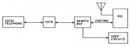
Fig. 1. PSTN operating mode diagram.
The box can be connected either to the Public Switched Telephone Network (PSTN) as in fig. 1, or at a local level with the circuit shown in fig. 2. It requires only the telephone and a few extra components. The station can be located in the garage, with the telephone the only radio "apparatus" in the family room. Add a speaker phone for general monitoring and use the handset for private conversation.
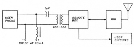
Fig. 2. Private line operating mode diagram.
Making it secure
After completing the hardware design, I addressed the issue of security. Could I limit transmitter access to ham operators only and maintain a reasonable amount of control during operations involving non-hams?
I solved the first problem by using an access code to activate the transmitter. To control operations involving non-hams, I decided to limit all communications from the telephone line to a 30 second maximum transmission time. If the telephone line carrier keeps the transmitter on past this time, the transmitter drops out and allows no further transmissions from the telephone until the box receives instructions from the control operator.
Operation
Begin operation by calling the remote unit from a remote telephone. After the selected number of rings you will hear the remote unit activate. You are now in the receive or monitor mode. Always listen for traffic already in progress before transmitting.
To transmit, enter your access code then press the # key and then the 9 key. After transmitting, depress the 9 key and the transmitter will deactivate. To transmit again, you need only hit the 9 key.
Terminate the call by hanging up or hitting the #; the remote unit automatically shuts down. Time-out timers allow transmissions of only 30 seconds or less.
Once the access code is entered, you can go into vox mode at the remote site by entering # and 0. The transmitter keys whenever you speak into the telephone. If the transmitter is keyed for longer than the allowed time, the remote unit will deactivate it and prevent further transmissions until the carrier from the telephone drops out and instructions are received from the control operator. To exit this mode enter # and 0 from the local site. This returns the remote to monitor mode.
Status indicators
Several indicators built into the software routines determine the status of the remote unit:
- CD - Main carrier detect.
- RADCD - Carrier detected is from the radio receiver.
- TELECD - Carrier detected is from the telephone line.
- OH - Remote unit is in the off-hook condition.
- PTT - Remote unit has the transmitter keyed.
- ACCESS - Remote unit has accepted access code.
Table 1 lists commands which activate specific output port pins. They are used to turn on NPN switching transistors that drive external control relays. These relays in turn activate additional functions through touchtones (DTMF) from a telephone or radio.
| Port A | |
|---|---|
| Output | bit-function |
| 1 | TELCAR |
| 2 | RADCAR |
| 3 | PTT |
| 4 | OH |
| 5 | SPARE |
| 6 | SPARE |
| 7 | SPARE |
| 8 | SPARE |
| Port B (User defined) | |
| Output | bit-function |
| 1 | #1 |
| 2 | #2 |
| 3 | #3 |
| 4 | #4 |
| 5 | #5 |
| 6 | #6 |
| 7 | #7 |
| 8 | #8 |
Mobile operation requires a touchtone generator. To call, enter your access code then send the * and 0 command to the remote unit. This takes the unit off hook and keys the transmitter for 3 seconds to acknowledge the dial tone. When the transmitter drops out, dial your number, listen for ring back and wait for an answer. The remote unit automatically goes into the vox mode. The operator has control of the remote unit and can terminate the call. Calls are limited to 3 minutes; all long distance calls are prevented.
Digital circuitry
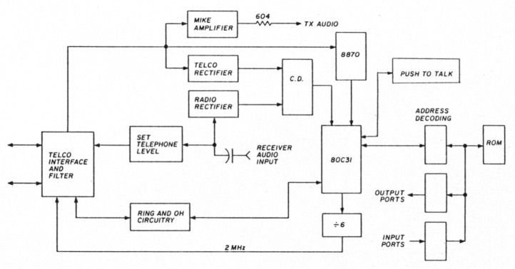
Fig. 3. Functional block diagram.
A microprocessor reduces the number of components (see the block diagram in fig. 3 and circuit in fig. 4). I used the 80C31 because of its timers, onboard RAM, interrupt structure, and special function registers. The 80C31 also has various op-code instructions which operate on internal and external bytes and bits for programming ease.
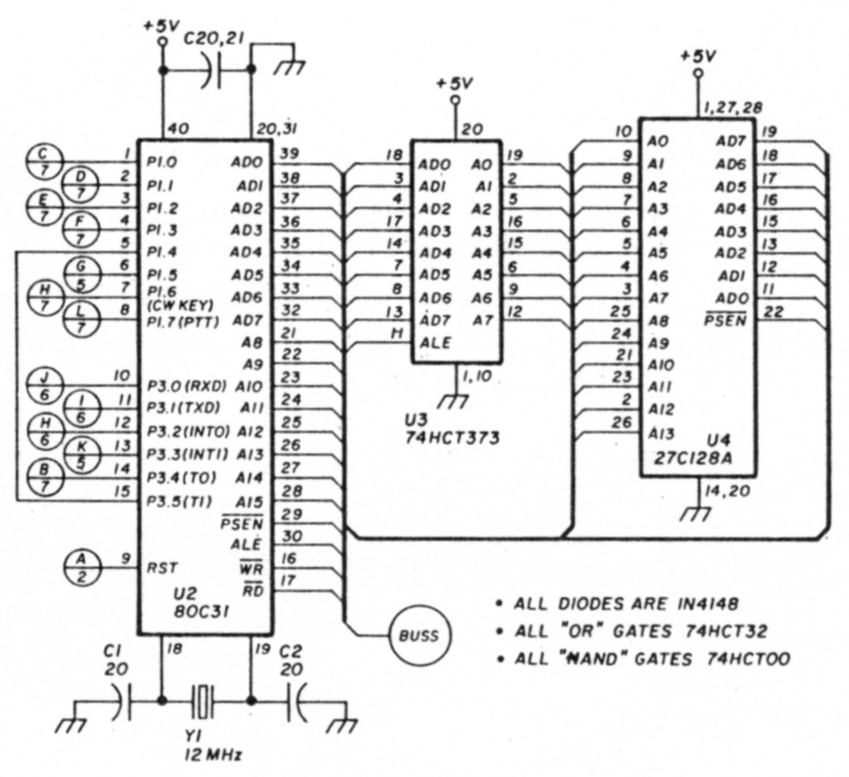
Fig. 4. "Brain" of controller is 80C31 microprocessor.
The microprocessor is configured as follows: Port 0 is used as a multiplexed port in conjunction with the 74HCT373 eight-bit latch to separate the lower order address from data. This occurs each time address latch enable (ALE) goes high. Port 2 serves as the higher order program address lines.
I selected this microprocessor, driven by a 12-MHz crystal, for its proper timer operation (which I will describe later). Port 1 serves as both the input and output port for the system. Port 1 bits, 0 through 3, are used as input data from the DTMF receiver. Port 1 bit 4 is used for an output pin for the 1-kHz clock, generated by the real-time clock routine in the software.
Port 1 bit 5 is used as an output control pin to make the off-hook (OH) relay active. This signal is generated when the unit is in private line (no dc), has detected the correct amount of ring cycles, or senses telephone line current. The tone generator is used for warning beeps and CW signal; Port 1 bit 6 is used to turn it on and off. Port 1 bit 7 is used as the push-totalk (PTT) signal to the radio transmitter whenever a transmission is requested.
Port 3 provides the system's interrupt scheme. Input pin 2 is an edge-triggered interrupt used for main carrier detection. Input pin 0, in conjunction with the main carrier detect bit, tells the microprocessor that the carrier is from the telephone lines. Input pin 1, along with the main carrier detect bit, tells the microprocessor that the carrier is from the radio.
Input Port 1 pin 3 is an edge-triggered interrupt that indicates the presence of a ring signal or telephone off-hook current.
Input Port 1 pin 4 tells the microprocessor that the carrier is a valid DTMF signal.
Input Port 1 pin 5, the input to a timer interrupt, generates a 1-second interrupt to drive the time-out timers and long delays. The remaining bits of Port 3 generate the system read and write signals.
The microprocessor reset is input on pin 9. A Dallas Semiconductor DS1232 is used as the reset and watchdog timer in this system. To prevent a reset signal from being generated, this reset circuit (fig. 5) must be written to by software at a periodic rate. A reset signal is also generated if the power drops below a predetermined level. This chip can save you trips to your remote site, but is not necessary for this application. A simple RC network can also be used to generate a reset signal on power-up.
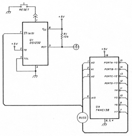
Fig. 5. Dallas Semiconductor DS1232 is used as reset and watch dog timer.
The program memory used is a 16K x 8 EPROM (27C128A), as seen in fig. 3, chosen to allow for expansion.
I needed extra input and output ports to provide for the input and output of control signals. The 74HCT138 is used to decode external addresses for these ports. Only four ports are used; four more-are held in reserve for expansion. All input and output ports (see fig. 6) use an eight-bit latch (74HCT373). Ports A and B are used for output; Ports C and D are for input.
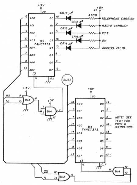
Fig. 6. Eight bit latches are used for input and output ports.
The write signal for the output ports (see fig. 7) is generated by the selection of an address, NOR'ed with the system write signal. This scheme is used for all external output ports. The read signal for the input ports is generated by OR'ing with the system read signal. Each input port bit is activated by opening the appropriate switch. The port pin is then pulled high by a pull-up resistor, telling the microprocessor it needs servicing.
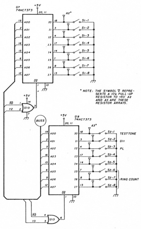
Fig. 7. User option inputs are determined switch settings.
DTMF signal decoding is done by the GTE 8870 CMOS DTMF chip (see fig. 8). Command signals may be entered into the system via the telephone line or radio receiver. When a valid DTMF signal is received, four bits are sent to the microprocessor input along with a strobe signal (std) telling the processor that the detected carrier is due to a DTMF signal. The processor then decodes this signal and performs the commanded task.
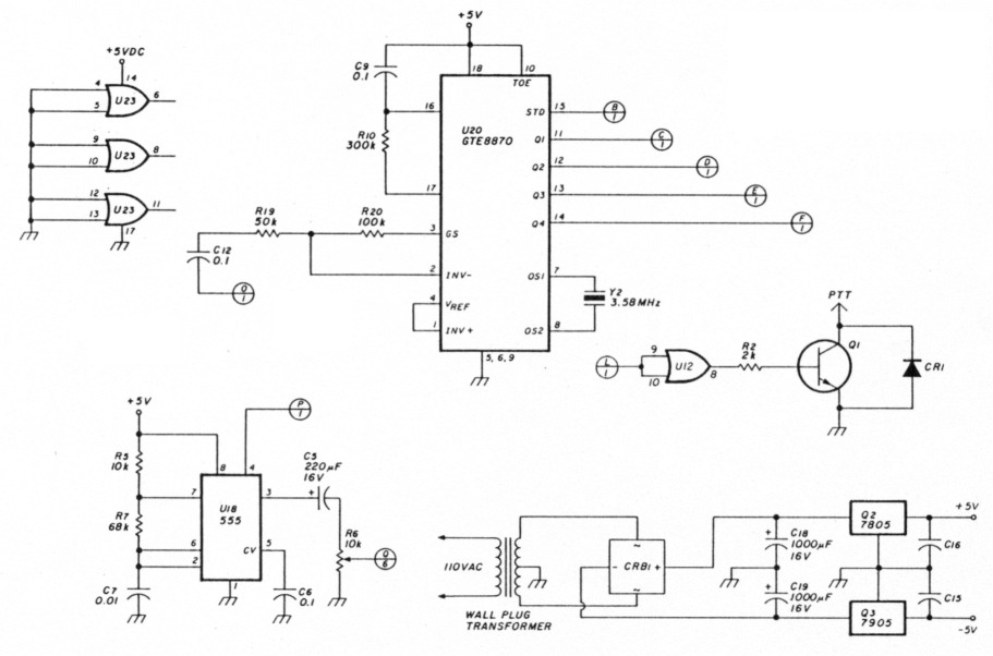
Fig. 8. A GTE 8870 is used as a CMOS DTMF chip.
The tone generator consists of a 555 timer chip, set for a frequency of 1 kHz. The generator is turned on by a signal from the processor. The signal is capacitively coupled and the level set by a 10-k pot - one of the inputs to a summing amplifier that supplies audio to the radio transmitter.
Analog circuitry
A description of the telephone interface circuitry (see fig. 9) begins with the ring and off-hook current components. The telephone network has a 600-ohm impedance, so transformer T1 is 600 to 600 ohms and meets FCC rules part 68: this box does not have FCC registration.
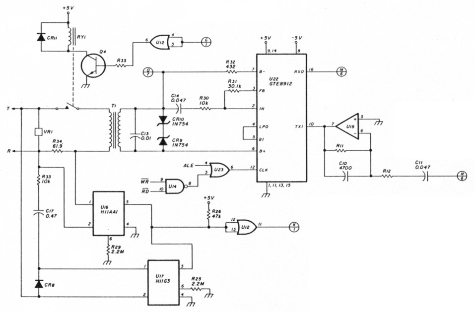
Fig. 9. Analog circuitry part of controller.
In an on-hook configuration, the dc path is broken by the off-hook relay. When a ring signal is applied across tip and ring, it is coupled through R33 and C17 from the ring side of the telephone line. The signal is then applied to the input of the H11G3 opto-isolator and CR8, and the ac circuit is completed through these components and tip side of the telephone line. When the ring signal goes positive H11G3 turns on, pulling resistor R26 low, generating an interrupt to the processor during each positive portion of the ring cycle. The processor requires a count of ten cycles out of every cycle for a good ring. Once the accumulated rings reach the count, selected by ring 1 through ring 3 dip switches on Port D, the processor sends a signal to the off-hook relay closing the dc path. This causes current to flow through the 61.9-ohm resistor, generating a voltage drop which turns the H11AA1 opto-coupler on. A signal is then sent to the processor indicating that line current is present. This signal is sampled continuously, and if line current disappears for a certain length of time the processor sends a deactivate signal to the off-hook relay.
The telphone line side of the interface has a device to protect it from the possiblity of over-voltage spikes. The secondary side of the telephone circuit has both transmit and receive signal currents. The GTE 8912 PCM filter splits the signal into either a receive or transmit path. Two zener diodes prevent the PCM filter from overloading.
The receive signal enters through C14 and R30, with the gain resistor being R31. The telephone output exits on pin 16 of the PCM filter. The radio receive signal enters the PCM filter on pin 10, and drives T1 through a differential amplifier in the PCM filter.
The DTMF receiver input is taken from the secondary side of T1, allowing command signals to be decoded from either the telephone or the radio receiver.
The PCM filter requires a 2-MHz clock signal to provide necessary filter characteristics. This signal is generated by first NAND'ing the system read and write signals, then OR'ing the result with the system ALE. As a result, the microprocessor clock frequency is divided by 6.
Audio and carrier detect
The telephone signal to be transmitted leaves the PCM filter at pin 16 and then enters through R22 into a summing amplifier, where the CW tones are also mixed when required (see fig. 10). The amplifier's output goes to the radio microphone input through a 604-ohm resistor serving as an impedance-matching device. This op-amp can be either an amplifier, attenuator, or buffer, depending on the ratio of R22 and R23. In my application it was a buffer.
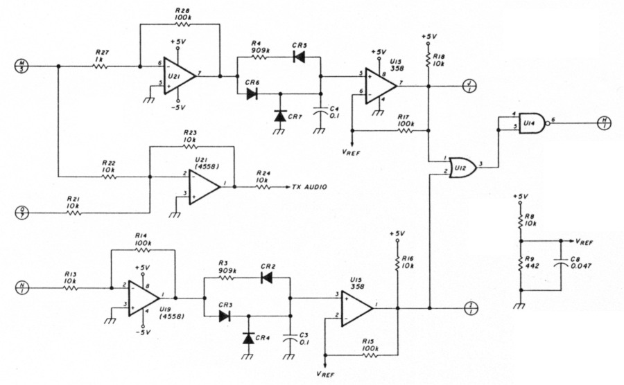
Fig. 10. Carrier detect circuitry.
The telephone carrier detect circuitry has three parts: signal amplifier, rectifier, and comparator. The amplifier takes the incoming signal and amplifies it to a level sufficient for rectification. The gain is then set by the R27 and R28 ratio. Diode CR6 half rectifies the signal allowing a positive voltage to be applied to the filter capacitor C4. Voltage is applied to the input on a voltage comparator, U15. When the voltage of the input signal rises above the voltage reference at pin 6, the output goes to a high state generating an interrupt through an OR gate. A signal is sent to the processor pin (described earlier) indicating the carrier is from the telephone. Resistor R17 provides a hystresis effect in the comparator stage, preventing output chatter if the incoming signal received is close in level to the reference. Diode CR5 and R4 are used to forward bias CR5. This discharges filter capacitor C4 which removes the signal from the processor. Carrier detection has a fast attack and a slow decay. CR7 prevents a negative voltage greater than 0.6 VDC from being applied to the comparator input. This will happen if the carrier stays off long enough - the circuit goes negative.
Radio receive signal path enters the system through C11 into a summing amplifier U19. This amplifier takes the signal from the radio and amplifies it to a -9 dBm output on the telephone line. Be sure your audio input level doesn't go above this level - it is the highest level permitted on the public switched system.
Approximately 35 mV is all that is required to achieve this level. I found the audio input to the volume control was the best method of obtaining audio from the radio receiver. This level should not be varied during normal operation.
The radio carrier detect circuit is identical to the telephone carrier detect circuit.
Strap option
Next select the parameters. Look over the functions of the Port C and D dip switches, and choose the ones for your application. (See Table 2.)
| Port C (SW-1) | Port D (SW-2) | ||
|---|---|---|---|
| Switch No. | Function | Switch No. | Function |
| 1-4 | First digit of access code 0-9 | 1 | Test of 1-kHz tone |
| 2 | Expansion | ||
| 3 | Private line (no dc) | ||
| 4 | Expansion | ||
| 5-8 | Second digit of access code 0-9 | 5 | Expansion |
| 6 | Ring count 0 (LSB) | ||
| 7 | Ring count 1 binary coded | ||
| 8 | Ring count 2 (MSB) | ||
Construction
Construction isn't critical; I've included the artwork double-sided pc board (figs. 11 and 12) and the component layout (fig. 13). I used components that were easy to obtain. You can order a printed circuit board or any major parts directly from me. I would be interested in any comments or ideas you may have; for a reply please enclose an SASE. I hope you have as much fun with this project as I've had.
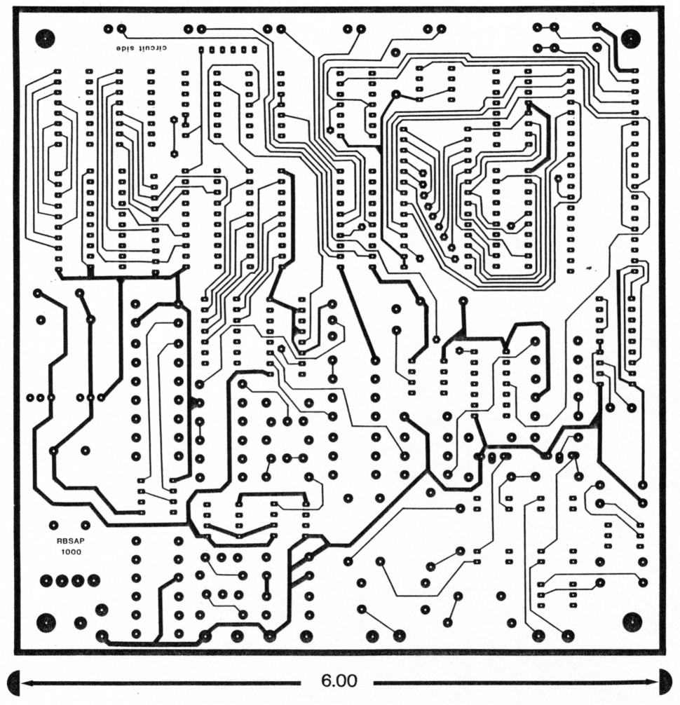
Fig. 11. Printed circuit board artwork - component side.
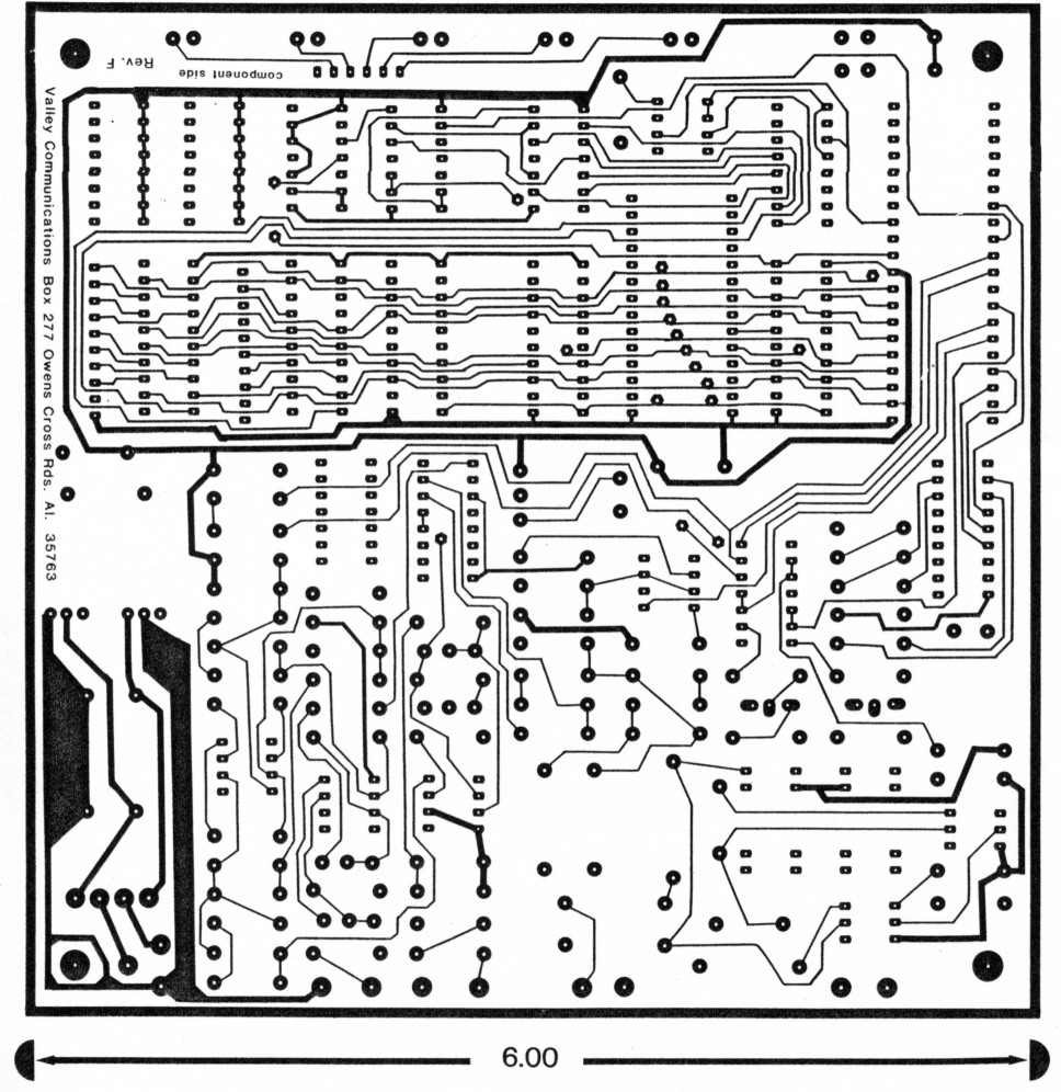
Fig. 12. Printed circuit board artwork - non-component side.
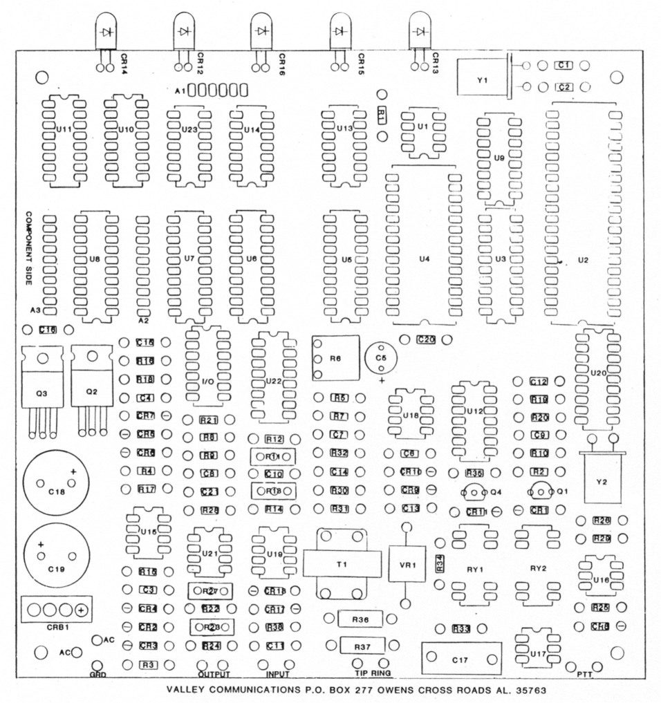
Fig. 13. Component layout superimposed on component side artwork.
AA4NX, Roger Owens and KK4LA, Jeff Owens.