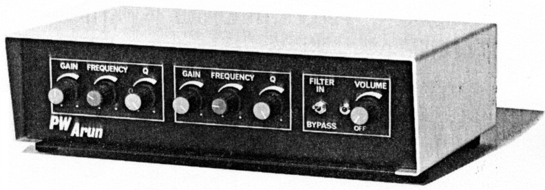
PW "Arun" parametric filter
Ben J. Duncan describes a powerful weapon in the audio processing armoury
The task of extracting a readable signal from crowded bands is usually looked upon as a matter of judicious adjustment of the various knobs controlling the r.f. parameters of a receiver. However, aside from the presupposition that the receiver in question sports a row of knobs to adjust, tweaking of the r.f. gain and i.f. filtering characteristics doesn't in itself guarantee readable reception. That's all part of the fun isn't it?
Less flippantly, a workable means of improving performance in this area is to process the audio output of the receiver. The advantages here are fourfold:
- Audio processing facilities can be added with little interruption to the wiring and aesthetics of the receiver, hence maintaining resale value.
- There are no worries about upsetting the finely tuned r.f. and i.f. sections of an elaborate set.
- Audio processing can improve the readability of signals on any receiver (even a domestic portable); it's not just limited to sophisticated communications receivers.
- Processing at audio frequencies per mits stable, sweepable filtering characteristics which are not easily achieved at r.f.
Filter Characteristics
Parametric filters, or "equalisers", are widely used in professional audio systems, but the term "parametric" is etymologically rather shaky and, in this context, has no connection with r.f. parametric amplifiers! Perhaps the best description of the filter is "A circuit in which each of three parameters that govern filter performance can be continuously varied". These are: amplitude, (GAIN, boost or cut), Q (or bandwidth) and centre FREQUENCY.
The possible manipulations are displayed graphically in Fig. 1. For comparison, the tone controls on a domestic hi-fi set up exhibit a fixed centre frequency and a Q that is both fixed and also very low, i.e. broad. Moreover, these controls tend not to hinge around a centre frequency, but instead, operate altogether either above (treble) or below (bass) a broad slab of midrange frequencies. By contrast, the parametric filter's "tunable and variable bandpass" scheme is ideal for homing in on a specific area of the spectrum, enabling potent treatment without undue effect on adjacent parts of the spectrum.
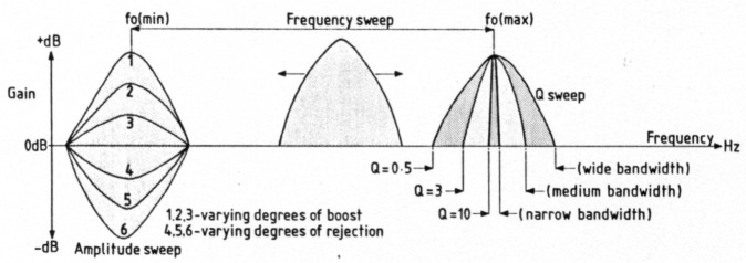
Fig. 1: The variation of three parameters is possible
Moving on to Fig. 2(a), the heart of the filter unit is a frequency selective circuit which is really just a "slugged" i.e. non-oscillating, version of the classic Wien-Bridge oscillator in disguise. Alternatively, the circuit can be approached as follows: Ignore for a moment R3 and R4 and imagine that the non-inverting (+) input of IC1 is earthed. The arrangement is now essentially that of the archetypal inverting amplifier, as shown in Fig. 2(b). Remembering for this circuit that the gain is given by R2/R1 - referring to Fig. 2(b), and then returning to Fig. 2(a), we can write the gain equation as (R2||XC2)/(R1 +XC1), where XC is the reactance of the capacitors at a given frequency. The effect of the series and parallel CR networks is to produce a frequency dependent peak in gain - in other words, a bandpass effect. The centre frequency (fo) of the gain peaking is given by: fo = 1/2πCR. Thus, by adjustment of either both C or both R values, we can alter the centre frequency. As a general rule, it's easier to alter the resistors.
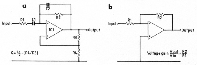
Fig. 2(a): Wien Bridge bandpass filter; (b) basic op-amp inverting amplifier
Going one step further, replacing R1 and R2 with a dual-ganged potentiometer gives us a sweepable centre frequency. Next, replacing R3 and R4 and connecting their centre tap to the op-amp's non-inverting terminal provides some controlled positive feedback to sharpen up the response curve. This equates to raising Q and the technique is much the same as applying positive feedback to improve the selectivity of an r.f stage, though it's not so finicky. Nonetheless, as is clear when you enter a few values into the Q equation, as Q approaches 10, the relative values of R1 and R2 in terms of setting Q become critical. For instance, if we make R3 equal 10kΩ, adjusting R4 to 18kΩ gives a Q of 5; with 19kΩ, Q is 10 and with 19.9kΩ, Q rises to 100! In this example, as R2 tends to 20kΩ, Q increases exponentially towards infinity, and oscillation becomes inevitable. Fortunately for audio applications, a Q in excess of 10 is not required and it is easy, with careful adjustment, to make the circuit perfectly stable with this Q value.
Circuit Description
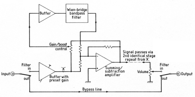
Fig. 3: Block diagram of the Parametric Filter
The block and circuit diagram of the PW Arun parametric filter unit are depicted in Figs. 3 and 4 respectively. Integrated circuit IC2b is configured as an inverting amplifier and has two purposes. In the first instance it buffers the circuitry, providing a low and predictable source impedance for succeeding stages, together with a high input impedance to avoid loading the receiver at the "take off" point. Secondly, it provides some gain to counter the reduction in level that occurs when the steep rejection facilities are in use and thereby helps to maintain the S/N ratio. At the same time, the exact degree of gain can be adjusted by R23 to suit the receiver's output level. Alternatively, R23 can be replaced by a fixed resistor once a suitable value has been determined. The gain of this stage is determined in the same fashion as for that shown in Fig. 2(b), in this instance equalling (R22 + the preset value of R23)/R21.
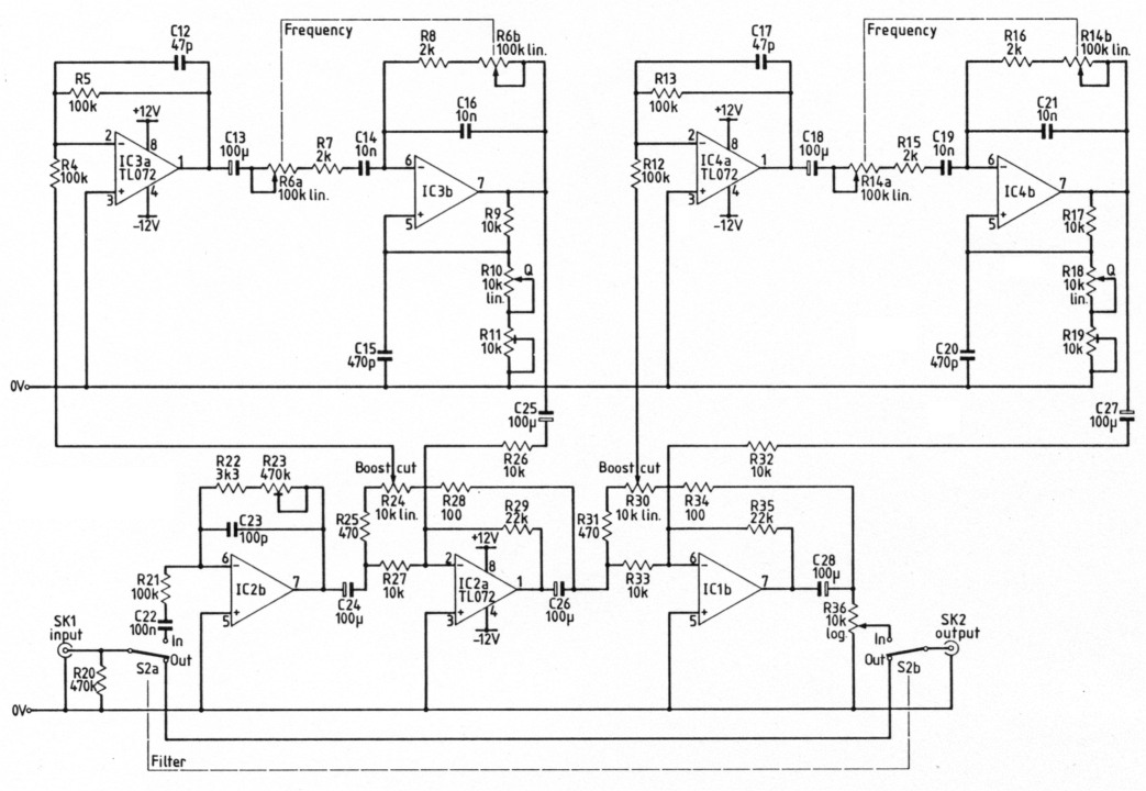
Fig. 4: Circuit diagram of the PW Arun Parametric Filter
As it stands, the Wien-Bridge band-pass filter examined in Fig. 2 can only boost signals at its centre frequency. In order to provide continuously variable boost and cut, the filter is placed in a feedforward/feedback loop configured around IC2a. With the slider of R24 towards R25, the circuit operates in the feedforward mode, and the properties of the Wien-Bridge filter (max. gain at fo) are reflected at the output of IC2a. As the slider of R24 is turned towards R28 negative feedback is progressively introduced, and after passing the centre point, further rotation causes the output of IC2a to decrease at fo. In other words, the Wien-Bridge filter's operation is inverted, and fo becomes the frequency of peak rejection. The overall result as the gain control is turned is continual gradation between signal boost and rejection referred to fo, with a null at the centre point, just like the operation of a tone control.
Looking more closely at the Wien-Bridge filter (IC3b and associated components), R7 has been introduced to prevent the preceding stage looking into a virtual short circuit when R6(a) is set at minimum. As both CR networks must be identical in value (otherwise Q will become unpredictable), R8 is added in series with R6(b) to maintain the relationship. Note that the value of R6 can't be much greater than 100kΩ to avoid spurious phase shifts (caused by stray capacitance across the pot and p.c.b. tracks) which would upset the circuit's h.f. stability and the predictability of setting up fo. With this in mind, it is clear that the stopper resistor R7 puts a limitation on the frequency range that can be swept by R6; i.e. min./max. frequency = (R7 + R6a + XC14)/(R7 + XC14). So in practice, even to cover the relatively narrow bandwidth of interest to radio communications, R7 must be made as low as is feasible. For this reason, a buffer amplifier, IC3a is placed ahead of the Wien-Bridge filter to avoid the severe loading that any practical value of R7 would place on the feedforward / feedback potentiometer, R24.
As we saw earlier, Q becomes critically dependent upon resistor accuracy as it approaches a value of 10. For this reason, a multi-turn preset is provided so that Q can be set up empirically to the highest stable value. The panel Q control then allows adjustment downwards from this point. Capacitor C15 is intended to remove the positive feedback at high (supersonic) frequencies. This is a wise precaution, as inevitable stray capacitances can all too easily give rise to uncontrolled positive feedback (hence oscillation), the effect becoming progressively more likely above 20kHz. Likewise, the phase margin on IC3a is increased by C12 to keep the whole loop well "tamed".
Most of the remaining body of the circuitry is simply iterative, being a second, wholly independent filter. Cascading two identical filters in this manner greatly increases the power of the unit to discriminate - one filter can be set to attenuate the interference, whilst the other is used to emphasise the important parts of the signal.
Moving on to the output, R36 controls the output level, whilst S2(a)/(b) provides a BYPASS function, allowing rapid comparisons between the filtered and unprocessed signal. This is partic ularly valuable when interference fades or signals drift.
The power supply (Fig. 6) is a little unusual in that a single regulator provides the split (± 12V) rails. Here, a spare op-amp in the dual package is used as an active potential divider, providing the +24V rail with an accurately balanced, low impedance centre tap. The resulting rails (0V, +12V and +24V) are then relabelled -12V, OV and +12V by sleight of hand!
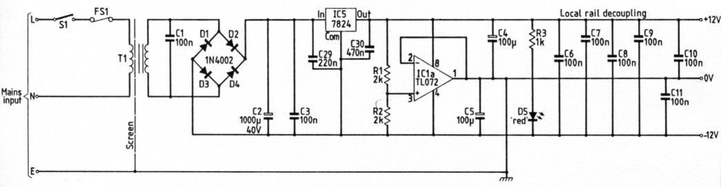
Fig. 6: Split-rail power supply details
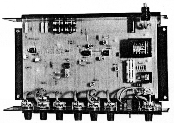
Construction Notes
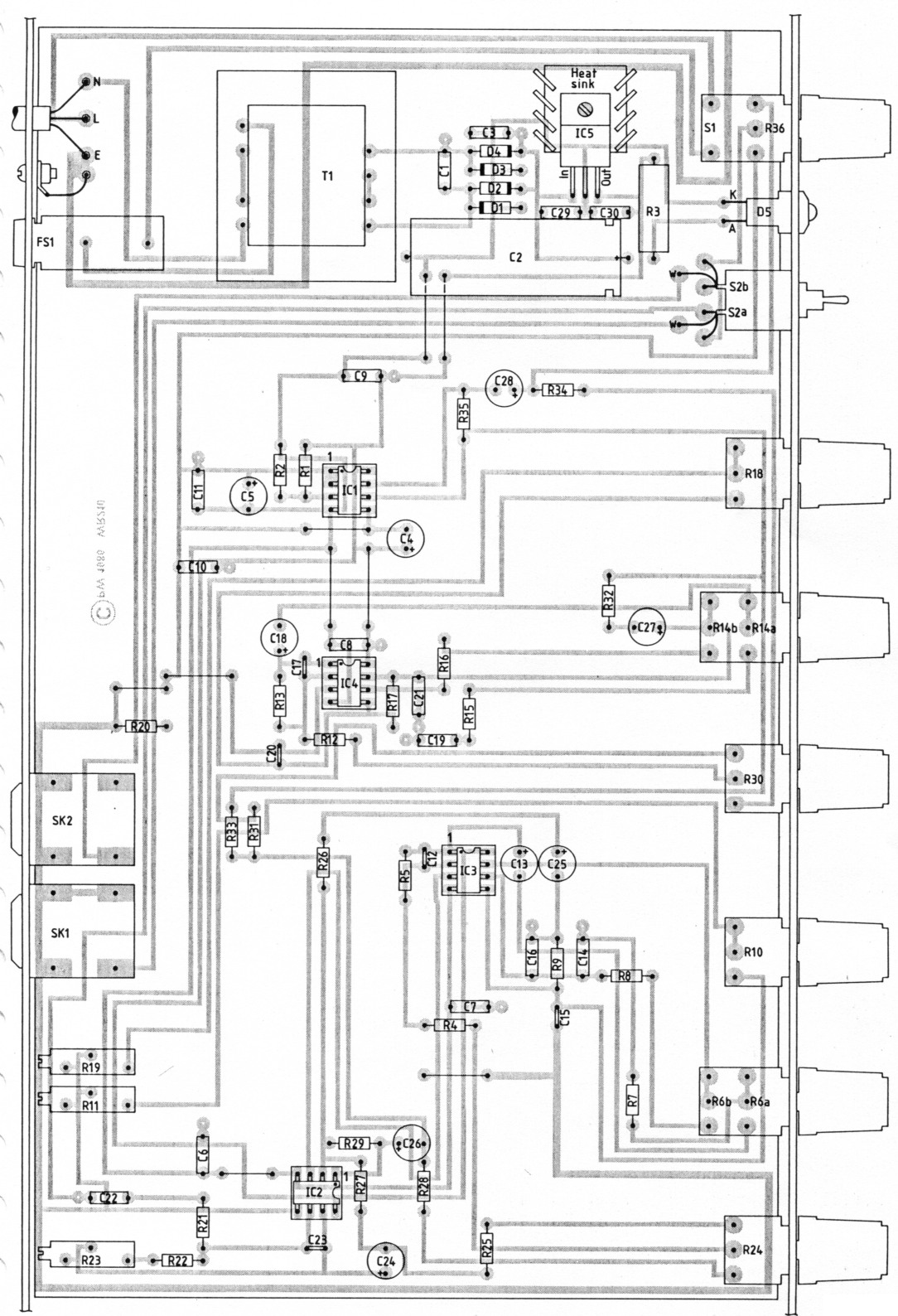
The filter unit is mounted entirely on a single p.c.b. By far the best method of assembly is to work in terms of ascending component height, mounting links, resistors and diodes first of all. Next, presets, capacitors (except C2) and the i.c. sockets. Take care to observe the polarity of C4 and 5; the other electrolytics can be mounted in either direction for the time being. Sockets for the i.c.s are recommended unless you have access to an efficient solder sucker - otherwise the correction of errors is likely to lead to p.c.b. damage.
The p.c.b. is designed to accept Radiohm p.c.b. mounting pots but readers may have difficulty finding this type. However, apart from the extra work of dressing a set of wires and fitting Veropins, the use of readily available tagged pots is altogether ac ceptable, providing the link wires are kept short, preferably less than 40mm. Likewise, the BYPASS switch can be either a p.c.b. mounting variety or any readily available miniature toggle switch. Again, the latter should be linked to the board via short tails.
On the topic of safety, the live tracks on the p.c.b. are wholly surrounded by a thick guard rail, connected to earth. This prevents the creepage of mains voltage to proximate tracks should the board ever become damp. It also ensures prompt rupture of the fuse if any significant leakage occurs. Additionally, a layer of blank glassfibre board should be screwed to the underside of the p.c.b. With this in place, it's virtually impossible to come into contact with live terminals accidentally, assuming of course that the mains terminal pins have been sleeved. Blank glassfibre is a waste product available for a nominal fee from p.c.b. manufacturers. Alternatively, a p.c.b. offcut lying around your shack can be quickly etched down to bare glassfibre. This completes assembly in so far as testing can commence.
Testing and Setting Up
Prior to testing the board, carefully check the polarity of C2/4/5, D1-4 and IC1-4. In addition, carefully check the pot and switch wiring.
Temporarily solder the mains cable to the p.c.b. pins and sleeve. Before fitting the glassfibre insulating board, carefully inspect the mains connections for minute slivers of stray wire or solder bridges capable of causing short circuits, then fit the glassfibre insulator. Finally, turn R6 and R14 to their centre positions; use a meter to determine this point, looking for a resistance reading of 50k0 or thereabouts.
Turn on at R36 and connect the mains. Check that l.e.d. D5 lights. If not, disconnect immediately and carefully check the power supply assembly. Assuming the l.e.d. lights, test for 30 to 36V across C2. Then test for the -12V and +12V rail voltages from pin 1 on IC1 to the negative and positive terminals of C2 respectively. This confirms the power supply is working. If not, inspect ICI a, R1/2 and associated connections.
We can now move on to checking the performance of the unit. If you own audio test equipment, then the test procedure will be self-evident. If not, it's perfectly possible to set up and assess the filter unit by ear alone. Connect a convenient source (a radio programme is best) to the input and a test amplifier or headphones to the output. If the headphone/external loudspeaker socket of the receiver is used to obtain the audio input ensure that a resistor of equivalent value to the phones/speaker impedance is wired across the jackplug. This will avoid any distress to the audio amplifier stages of the receiver. With switch S2 set to BYPASS there should be normal reproduction. Set the Q controls R10/18 at minimum (fully anticlockwise) and the boost/cut GAIN controls R24/30 at their central positions. Move S2 to FILTER IN and adjust VOLUME control R36 for a comfortable level. Turn R24 to max (fully clockwise) and sweep the FREQUENCY control R6, listening for a corresponding "squawky" enhancement of the programme around the centre of the sweep. Next, turn the Q control RIO to maximum and note the sharper effect when the frequency is swept again. Repeat the same process with R24 set at minimum, noting the "hollow" sound as R6 is swept through the midrange frequencies. The Q preset R11 should now be turned clockwise a couple of turns. Test all three controls over their whole range, listening for oscillation or severe ringing (impulsive sounds are drawn out with a pipe-like quality when this occurs). Progress another two turns and test again. When oscillation occurs, first turn down R36 (to avoid hurting your ears!) and then turn back R 11 until the circuit restabilises at all control settings. If you have a 'scope, it's a good idea to check that there's no supersonic oscillation - it's absence is a good sign that the circuit is stable.
Repeat the same procedure with the second filter, R14, 19, 30. At this point, it's possible for slight interaction to occur, insofar as the stable Q setting on the first filter now causes problems at certain control settings. However, this is quickly solved by tweaking R 11 and R19 half-a-turn anticlockwise at a time, until the problem ceases.
If intractable oscillation does occur, even with R11 and R19 set at or near minimum (fully anticlockwise), this almost certainly indicates a circuit fault, such as an incorrect resistor or pot value. However, it's also worth empirically adjusting the values of C12, 15, 23 (etc) by ± 100 per cent to counteract the effects of a freak combination of component tolerances. Next, switch off the unit and test the voltages with respect to OV (pins 1 and 2 on IC1 a on C13, 18, 24, 25, 26, 27 and 28. Swap these around where necessary to accommodate the polarity of the offset voltage appearing from the preceding stage. If the offsets are less than 0.1V, reversed electrolytics will come to no harm, and are best left alone. Conversely, offsets greater than 1V should be investigated, as they indicate a circuit fault, possibly an open circuit bias resistor or faulty op-amp.
One more adjustment remains to be made. Once the filter unit is wired to your receiver, adjust R23 to provide a signal level that's commensurate with audibility (with both filters in the maximum reject mode), and a clean response (with the filter at its maximum boost settings), not forgetting the ability of the gain control in the receiver and R36 to optimise the dynamics in everyday use.
| Resistors | ||
|---|---|---|
| 100Ω | 2 | R28,34 |
| 470Ω | 2 | R25,31 |
| 3.3kΩ | 1 | R22 |
| 10kΩ | 4 | R26,27,32,33 |
| 22kΩ | 2 | R29,35 |
| 100Ω | 5 | R4,5,12,13,21 |
| 470kΩ | 1 | R20 |
| 2kΩ 1% Metal film | 6 | R1,2,7,8,15,16 |
| 10kΩ 1% Metal film | 2 | R9,17 |
| 1kΩ 1 W 5% | 1 | R3 |
| Potentiometers | ||
| 10kΩ Cermet multi-turn trimmer | 2 | R11,19 |
| 470kΩ Cermet multi-turn trimmer | 1 | R23 |
| 10kΩ lin | 4 | R10,18,24,30 |
| 10kΩ log with s.p.s.t. switch S1 | 1 | R36 |
| 100kΩ lin dual | 2 | R6,14 |
| Capacitors | ||
| 100nF | 9 | C1,3,6-11,22 |
| 220nF | 1 | C29 |
| 470nF | 1 | C30 |
| 10nF 5% | 4 | C14,16,19,21 |
| 47pF | 2 | C12,17 |
| 100pF | 1 | C23 |
| 470pF | 2 | C15,20 |
| 100pF 16V radial | 9 | C4,5,13,18,24-28 |
| 1000µF 40V axial | 1 | C2 |
| Semiconductors | ||
| 1N4002 | 4 | D1-4 |
| Red I.e.d. | 1 | D5 |
| TL072 | 4 | IC1-4 |
| 7824 | 1 | IC5 |
| Miscellaneous | ||
| Printed circuit board; | ||
| fuseholder, 20mm p.c.b. mounting with 160mA antisurge fuse | ||
| 6mm mono jack socket | 2 | |
| transformer, 240V p.c.b. mounting, 12-0-12V, 6VA (RS 207-756) | ||
| miniature toggle switch, d.p.d.t. | ||
| control knobs | 7 | |
| case | ||
| 8-pin d.i.l. sockets | 4 | |
| Veropins | ||
Specification
| Frequency response | -3dB @ 15Hz and 16kHz |
|---|---|
| Gain swing | +15dB, -20dB per |
| Q range | 0.5 to 10 (typical) Filter |
| Centre frequency range | 150Hz to 6kHz stage |
| Maximum output level | +18dBm (6V r.m.s.) |
Ben J. Duncan.