The Microwave MESFET 1
Plessey gallium arsenide m.e.s.f.e.t. device
MESFETS are the simplest form of amplifier device available for higher frequencies, says Brian Dance as he unravels some of the mystery surrounding these devices.
In spite of the enormous success of the silicon planar transistor, this device has very definite limitations when it is used at higher and higher frequencies. Such conventional transistors are known as bipolar types, since the current flows in both p-type and in n-type semiconductor material as it passes through the device. The limitations on the performance of such devices as the frequency rises through values of a few GHz is so serious that it soon became clear another type of device was needed for use in such frequency regions.
The fabrication of the first gallium arsenide m.e.s.f.e.t. (metal semiconductor field effect transistor) in 1964 proved to be the most significant breakthrough. The initial development of m.e.s.f.e.t. devices was slow, but then intensive research on these devices was undertaken to satisfy the need for light-weight, low-power, high-reliability devices able to replace travelling wave tubes at frequencies of up to some tens of GHz where bipolar transistors are useless.
The research resulted in a rapid improvement of the performance of commercial m.e.s.f.e.t. devices and types are now available which can be used at frequencies of up to about 60GHz. Initially the main applications were in the military and satellite fields where costs are not so restrictive as in many other fields. Unfortunately microwave m.e.s.f.e.t. devices are considerably more expensive than bipolar transistors and therefore the latter are still used for the less demanding applications at frequencies of up to about 5GHz. The simplest form of amplifier device available for higher frequencies, m.e.s.f.e.t.s are also used at frequencies of about 1GHz upwards where the highest possible performance is required.
It seems almost certain the m.e.s.f.e.t. devices will be widely employed in ground stations for the low-noise reception of television signals in DBS systems. This will create a far larger market for m.e.s.f.e.t. devices and should result in a very substantial lowering of prices. Small signal m.e.s.f.e.t. devices are available which can provide both higher gain and lower noise amplification than bipolar types at increasingly higher frequencies. Other m.e.s.f.e.t. devices can provide moderate power output levels at somewhat lower frequencies.
Internal Structure
The internal structure of a m.e.s.f.e.t. device is shown in Fig. 1. 1 . The current flows only through the thin n-type layer and therefore m.e.s.f.e.t.s are unipolar devices. The main advantage of selecting a unipolar device is that the charge storage in the base region of a conventional bipolar transistor is eliminated. It is this charge storage which mainly limits the high frequency performance of bipolar devices.
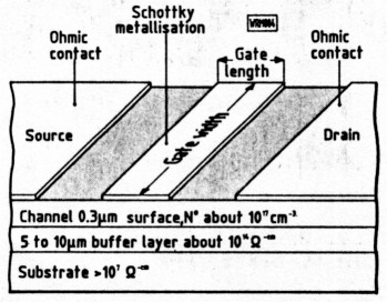
Fig. 1.1: Internal structure of a m.e.s.f.e.t. device
The construction of individual m.e.s.f.e.t. devices varies considerably from one type to another, but the thin n-type channel of Fig. 1.1 has a typical thickness of 0.3 micron and contains 10" impurity atoms per cm3. It is deposited on a high resistivity buffer layer (which may have a thickness of about 10 micron). The buffer layer is formed on a substrate of much lower resistivity.
The gate is a metal electrode, not a semiconductor material. A Schottky metal to semiconductor junction is formed by the gate, so the acronym m.e.s.f.e.t. may also be interpreted as metal Schottky field effect transistor.
The gate potential controls the width of the channel in the thin n-type layer, and this potential can therefore be employed to control the number of charge carriers flowing in the channel; this determines the current flowing between the source and drain.
As m.e.s.f.e.t.s are depletion devices, the gate potential is made more negative, the channel becomes narrower until eventually the gate is sufficiently negative to close the channel completely with the result that the drain-tosource current is cut-off.
The high frequency performance and hence the maximum practical operating frequency of a m.e.s.f.e.t. is dependent mainly on the channel length. The smaller the channel length, the lower the stray capacitance and the higher the maximum frequency of operation. The channel length is determined mainly by the length of the gate electrode shown in Fig. 1.1. Unfortunately it is very difficult to manufacture m.e.s.f.e.t. devices with very short gate lengths by conventional photolithography, especially if price considerations dictate that a high yield of successful devices must be obtained. Electron beam lithography is now often used, but the use of such new techniques inevitably raises costs, so it. is used only for devices to be operated. at the higher frequencies.
In general, gate lengths of about 1 micron have been widely used for devices designed to operate at frequencies of the order of 4GHz, such as those in satellite receiver ground stations. A gate length of 0.5 micron is more suitable for m.e.s.f.e.t. devices intended for operation at 10-15GHz, whereas gate lengths around 0.2 micron or less are appropriate for frequencies of over 20GHz. Unfortunately the fabrication of devices with such gate lengths is quite difficult.
Apart from the increase in the maximium operating frequency, the reduction of the gate length of a device tends to produce an improved signal-to-noise ratio at any given frequency. The gate length is therefore one of the most important parameters of a m.e.s.f.e.t. device.
Designed for the production of appreciable power at microwave frequencies, m.e.s.f.e.t.s have the same basic internal construction as that used in low power devices, with a similar gate length. However, the gate width is greater in power devices and it is important to minimise the thermal resistance from the device junctions to the case to prevent an excessive temperature rise. The maximum output power obtainable from the latest commercial devices at any given frequency has steadily increased year by year during the past decade and the noise figures of these power devices have also been steadily reduced. However, as the frequency of operation increases, it becomes far more difficult to obtain even a moderate amount of output power.
Materials
The best m.e.s.f.e.t. devices are fabricated in gallium arsenide, although m.e.s.f.e.t. devices can be produced more economically in silicon. Gallium-Arsenide is not only a much more expensive material than silicon, but it is far more difficult to work with. A silicon surface can be easily oxidised to form a passivating layer of silicon dioxide which prevents the ingress of contaminants, whereas gallium arsenide cannot be passivated in this way. Gallium arsenide is very brittle, so that much thicker wafers of this expensive material must be used than in the case silicon processing. In addition, the proportion of gallium arsenide m.e.s.f.e.t. devices produced which perform satisfactorily is much lower than in the case of silicon based products.
One of the main attractions of gallium arsenide is the high electron mobility of about 8000cm/Vs which is over five times that of silicon (1500cm/Vs). This high electron mobility is the main reason why gallium arsenide m.e.s.f.e.t. devices offer a better high frequency performance than comparable silicon devices. The electrons carry the current in the n-type channel of Fig. 1.1. It may be noted that hole mobility in gallium arsenide is lower than that in silicon; gallium arsenide m.e.s.f.e.t.s for high frequencies are therefore always n-channel devices, since the performance of p-channel devices would be limited by the hole mobility in the p-type channel. Gallium arsenide is not normally used to fabricate bipolar transistors, since the minority carrier lifetime in this material is about 250 000 times less than in silicon and very few of the minority carriers in the base region would reach the collector. However, minority carriers play no part in m.e.s.f.e.t. operation and have no effect on gallium arsenide m.e.s.f.e.t. performance.
Gallium arsenide is currently employed in all m.e.s.f.e.t. devices which must provide an optimum performance. However, a silicon-on-sapphire technique has been developed by General Electric of New York for fabricating m.e.s.f.e.t.s which can provide a moderate output power of under 1W at a frequency of up to 3GHz. These silicon-sapphire m.e.s.f.e.t.s can be produced more economically than gallium arsenide devices, it may also be possible to integrate them into monolithic silicon circuits.
Bipolar Comparison
In order to compare the performance of typical bipolar silicon high frequency transistors with that of gallium arsenide m.e.s.f.e.t. devices, we will consider the typical noise figures and gain values which can be provided by these two types of device. However, it must be made clear that each product is designed for a certain frequency range, while some types are designed for low-cost applications where a sacrifice in performance must be accepted. Thus these considerations must be borne in mind and not just the device performance alone.
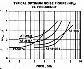
Fig 1.2
The variation of the noise factor for typical devices from the Avantek range of bipolar transistors with frequency is shown in Fig. 1.2. The AT-0017A (which is suitable for operation only at relatively low frequencies) and the AT-00135 are from this manufacturer's general purpose range of silicon bipolar devices, whereas the other devices are from the low noise range. It can be seen that the typical noise figure rises rapidly with increasing frequency until the devices are of little use for low noise reception.
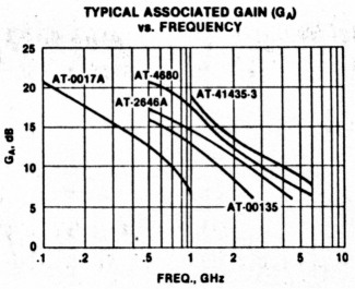
Fig 1.3
The typical associated gain of these Avantek devices falls with increasing frequency as is shown in Fig. 1.3. Again the performance of the bipolar devices falls rapidly with increasing frequency. The optimum noise figure for two m.e.s.f.e.t. devices from the same manufacturer is shown in Fig. 1.4 The AT-811 I is a small signal ultralow-noise gallium arsenide device designed for operation in the 2-6GHz region. The AT-8251 is an ultra-lownoise medium-power gallium arsenide m.e.s.f.e.t. intended for use in the 2-12GHz range. It can be seen that the noise figure of both of these devices is very low throughout the frequency range for which they are designed to operate. The decrease of the associated gain of these devices with increasing frequency is shown in Fig. 1.5.
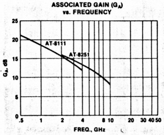
Fig 1.4
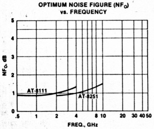
Fig 1.5
Noise Figure
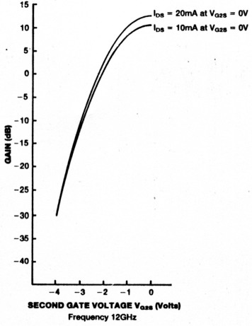
Fig 1.6: The variation of the gain with the second gate voltage at 12GHz.
It must be made clear that the noise figure of a device depends on the bias and other circuit conditions employed. The values quoted are those obtained under optimal conditions. Even at 30GHz noise figures are now approaching 2dB, while at 18GHz they are about 1.4dB and at 4GHz about 0.25dB in the best m.e.s.f.e.t. circuits.
Devices are available with short gate lengths which have fT (transition frequency where the gain is unity) of about 100GHz. Such devices can be used as oscillators at frequencies of up to some 80GHz.
Plessey Semiconductors has introduced a dual-gate gallium arsenide m.e.s.f.e.t. device, the P35-1310, in which the second gate can be employed for automatic gain control. The variation of the gain with the second gate voltage at 12GHz is shown in Fig. 1.6. The noise figure and the associated gain of this device are plotted against the drain-to-source current, Ips in Fig. 1.7.
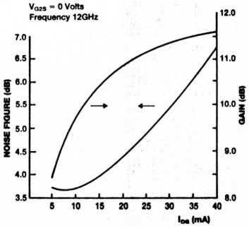
Fig 1.7: Noise figure and associated gain against drain-to-source current
Gallium arsenide m.e.s.f.e.t. devices used at ambient temperatures can provide a noise performance equivalent to a noise temperature of about 70K in the 4GHz region. The noise level can be reduced to about 55K by cooling the m.e.s.f.e.t. device with a thermo-electric cooling device, but this involves the consumption of power a vital point in amplifiers used in a satellite. Parametric amplifiers can offer noise temperatures of somewhat under 50K even when not cooled, whereas cooled parametric amplifiers can offer noise temperatures of 30K for thermoelectric cooling or under 15K for cooling by liquid gases. Still lower noise temperatures can be obtained by using a maser, but this involves liquid helium cooling in complex equipment and a reduced bandwidth.
Handling and circuit precautions
Gallium arsenide m.e.s.f.e.t. devices require careful electrical handling. Unlike m.e.s.f.e.t. devices, there is no insulating dielectric between the gate and the channel. A small potential across the Schottky gate structure can cause large currents to flow between the metal gate electrode and the semiconductor material below it. As the gate has very small dimensions, this will almost certainly result in the fusing of the gate electrode and the destruction of a relatively expensive device. This is not surprising, since it can be shown that even a small current can produce a current density in the region of the gate electrode of the order of a million amps per cm2.
The gate electrode must never be allowed to become positive with respect to the channel. Care must be taken to ensure that the bias voltage is applied to the gate before the power is applied to the circuit generally. In general it is desirable to use separate positive and negative power supply lines to bias the drain and gate electrodes separately.
In addition, gallium arsenide m.e.s.f.e.t. devices can be easily destroyed by the electrostatic charge accumulated on the gate electrode of the device. It is wise to be safe and to ground anything before it is allowed to touch the device. The leads of devices not currently in use should be shorted together.
Care should be taken to ensure that any soldering iron used to solder m.e.s.f.e.t. devices into a circuit is properly grounded and the soldering time should be minimised. Before attempting to solder the device into a circuit, the points to which it is to be connected should be grounded.
Power MESFETS
The output power which a single gallium arsenide m.e.s.f.e.t. can provide is limited to about 1W for each 1 mm of the gate width for optimally designed devices and circuits over the 4-15GHz frequency range. In practice this means that using current technology one can obtain about 10W output from a device at frequencies of several gigahertz and about 4W at 10GHz. The output can be increased somewhat by using a number of m.e.s.f.e.t. devices in parallel; thus some 40W of output power can be obtained at several gigahertz.
If one requires higher power levels of some hundreds of watts, one will normally use travelling wave tubes rather than m.e.s.f.e.t.s. Apart from the greater power level required by the travelling wave tube to heat the cathode, etc., the reliability of travelling wave tube is considerably worse than that of m.e.s.f.e.t. devices and these factors can be of great importance in satellite borne equipment. Even in low power m.e.s.f.e.t. devices, one can expect the mean time between failures to increase by a factor of about 2 for each 10°C fall in the channel temperature.
Although output power levels from gallium arsenide m.e.s.f.e.t. devices can reach about 1W at 20GHz the available output power falls rather rapidly with increasing frequency. When one leaves the microwave region and passes into the millimetre wavelength frequency region at about 30GHz, m.e.s.f.e.t. devices are unsuitable for the generation of appreciable power and travelling wave tubes are normally employed.
Each year the maximum power level available at any frequency using m.e.s.f.e.t. devices rises and the picture may alter considerably in the next few years.