The HEMT - A very high performance microwave device
There is a great need for very low noise amplifying devices which can operate at microwave frequencies in satellite receivers, military equipment and in various other applications. So Brian Dance takes a look at the high electron mobility transistor - or h.e.m.t.
In many cases it is important that these very low noise amplifying devices used should be able to provide a low noise performance in room temperature operation so as to avoid the need for a supply of liquid nitrogen or even liquid helium. The microwave m.e.s.f.e.t. (metal semiconductor f.e.t.) in gallium arsenide has met such needs for some years, as it provides excellent characteristics for low noise amplification at frequencies up to about 20GHz or even more.
HEMT/MESFET Comparison
After the introduction of a special type of f.e.t. known as the h.e.m.t. (high electron mobility transistor) in 1979, the microwave world has found this device to be an increasingly attractive competitor to the m.e.s.f.e.t. The h.e.m.t. is especially useful at frequencies of the order of some tens of GHz where the limitations of the m.e.s.f.e.t. became more apparent.
The structure of the h.e.m.t. is basically similar to a m.e.s.f.e.t. in which an improved performance is obtained by specially formed layers of more than one type of semiconductor material. Thus h.e.m.t.s are more expensive to produce than m.e.s.f.e.t.s and are therefore unlikely to displace them at frequencies of a few GHz or less unless noise considerations are exceptionally critical.
One of the most important parameters affecting the performance of both m.e.s.f.e.t. and h.e.m.t. devices is the gate length (typically a fraction of a micron). It is very difficult and costly to fabricate devices with the extremely short gate lengths required for optimum low noise performance at the highest frequencies. The cost of such high frequency devices is increased further because the proportion of short gate length devices in each batch which have to be rejected is greater than in the case of devices with longer gates for lower frequencies. At the present time, state-of-the-art gates 0.25pm in length can be produced by electron beam lithography; this involves the use of an expensive machine which takes time to write each individual device pattern. The price for h.e.m.t.s are currently of the order of a few tens of pounds per device.
The more expensive devices are therefore reserved for applications where very low noise performance is required at the highest frequencies. In general the performance of a h.e.m.t. with a 0.5µm gate length is comparable with that of a gallium arsenide m.e.s.f.e.t. of half the gate length.
A further advantage of the h.e.m.t. over the m.e.s.f.e.t. is its lower power dissipation which can be of considerable importance in some satellite communications applications.
HEMT devices are now available commercially, especially from various Japanese manufacturers. Fujitsu of Tokyo originally developed the h.e.m.t. and owns the name `h.e.m.t.' in Japan, but some others have marketed the devices as 'hetero-junction f.e.t.s'. Other names for the h.e.m.t. include the m.o.d.f.e.t. (MOdulation doped f.e.t.), the t.e.g.f.e.t. (Two dimensional Electron GaAsf.e.t.), the h.i.f.e.t. (Hetero-Interface f.e.t.) and the s.d.h.t. (Selectively Doped Heterostructure Transistor).
Construction
The h.e.m.t. structure is basically similar to that of a m.e.s.f.e.t. and involves a source, a drain and a Schottky gate. Although the gate potential regulates the current flow between the source and the drain as in a m.e.s.f.e.t.. It is the difference in the layers of the underlying semiconductor materials which distinguish the h.e.m.t. from the m.e.s.f.e.t. and which provides its improved performance.
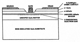
Fig. 1: The construvtion of a typical h.e.m.t. device.
The construction of a typical h.e.m.t. device is shown in Fig. 1. It contains a lattice-matched hetero-junction between two compound semiconductors (often gallium arsenide and gallium aluminium arsenide). The crystal lattice must be closely matched to minimise lattice strain, aluminium gallium arsenide having a lattice spacing within 0.1% of that of gallium arsenide. extremely abrupt hetero-junctions can be grown by such techniques as molecular beam epitaxy (m.b.e.).
Electrons from the donor silicon atoms in the aluminium gallium arsenide layer can move through the crystal until they fall into the lowest available energy states. In the h.e.m.t. device these energy states are in the gallium arsenide close to the hetero-junction interface.
This results in the accumulation of electrons in an extremely thin layer which has a thickness of less than l0nm. The electrons are said to form a two dimensional electron gas. Thus the h.e.m.t. is a quantum semiconductor device. There are no donor atoms intentionally present in the undoped gallium arsenide layer, so the electrons in the two dimensional electron gas do not undergo impurity scattering.
High Mobility
Therefore they have a greater mobility than electrons in a piece of bulk gallium arsenide, namely about 6500cm2/V-s at 300K, corresponding to a velocity of about 2 × 107cm/s. This is about twice the mobility of electrons in a m.e.s.f.e.t. (Mobility is the speed at which they move under a given electric field). In a h.e.m.t. cooled in liquid nitrogen, the mobility increases to some 80 000cm2/V-s (depending on the epitaxial structure).
The gas forms because of the greater affinity of the electrons for the positive undoped gallium arsenide layer. The two dimensional gas forms the carrier channel between the transistor source and the drain. The low noise of the h.e.m.t. relative to a m.e.s.f.e.t. of similar gate length is believed to be due to the two degrees of freedom of the electron in a h.e.m.t. as compared with three degrees of freedom in the m.e.s.f.e.t. Thus there is less random motion of the electron flow in a h.e.m.t. and this leads to less noise.
The mobility of the electrons may be further increased by employing a thin layer of undoped aluminium gallium arsenide adjacent to the hetero-junction interface. This layer provides more separation between the electron gas and the ionised centres which scatter the electrons and therefore reduce their mobility.
The structure of the h.e.m.t. produces not only higher electron mobility, but also a higher sheet carrier density (of the order of 1 × 10¹² per cm2) and a higher saturation velocity. These factors result in the h.e.m.t. having a higher transconductance and a lower noise figure than gallium arsenide m.e.s.f.e.t.s with comparable gate lengths.
The Gate
A Schottky barrier gate, implanted on top of the doped layer, is used to control the number of electrons in the two dimensional channel via depletion or enhancement. A bias applied to the Schottky barrier gate can be used to modulate the number of electrons in the channel and hence can control the conductivity of the device.
In contrast to the operation of the normal f.e.t., the width of the channel remains fairly constant in a h.e.m.t., but the number of carriers present is modulated. Hence the alternative name of m.o.d.f.e.t. for the h.e.m.t. Electrons in a h.e.m.t. move in the very thin layer, travelling parallel with the hetero-junction interface.
It is possible to manufacture both enhancement and depletion mode h.e.m.t. devices by suitable gate nrctallisation, layer thicknesses and doping levels. A feature which renders h.e.m.t.s particularly attractive for the future is their planar structure, which should enable them to be easily made by conventional silicon v.I.s.i. processing methods.
As in other high frequency f.e.t. devices, it is essential to employ a very short gate length to obtain low noise at high microwave frequencies.
One might expect a still better performance from h.e.m.t.s at low temperatures, since the two dimensional electron gas mobility at 77K is about 60 000cm2/V-s. Unfortunately, low temperature h.e.m.t. performance is affected by deep electron traps.
Performance
The noise figures of h.e.m.t. devices manufactured by Toshiba are compared with some of the company's m.e.s.f.e.t. in Fig. 2. It can be seen that the h.e.m.t. devices generally offers a lower noise figure than m.e.s.f.e.t. devices at the same frequency. The S8902 and the S8901 have gate lengths of 0.3µm and the S8900 is 0.25µm.
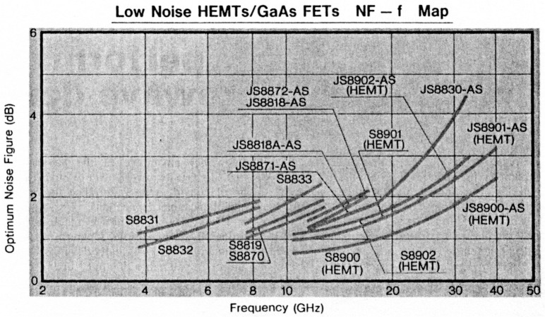
Fig. 2: The noise figures of Toshiba h.e.m.t. devices.
Although the h.e.m.t. devices will operate at higher frequencies with lower noise than the corresponding m.e.s.f.e.t. devices, h.e.m.t.s are more costly and their short gate length necessitates a reduced power handling capability. Toshiba is hoping to develop indium gallium arsenide h.e.m.t.s with noise levels about 0.6dB at 12GHz, but they are not expected to be available until later this year.
Type Examples
The Fujitsu FHR01FH 'ultra low-noise' h.e.m.t. device uses a 0.5pm gate length to obtain noise figures comparable with those of m.e.s.f.e.t.s which have 0.25µm gate lengths. The FHR01FH has a maximum noise figure of 2dB (typical 1.8dB) at 20GHz with a typical associated gain of 8dB. An FH package developed for the device allows it to operate at up to 22GHz without parasitic resonances. Noise figure and gain are shown in Fig. 3. At a temperature of 50K, the noise figure is typically 4.7dB at 20GHz. Maximum drain-source voltage sting is 3.5V. The transconductance is typically 20mS with a drain-source voltage of 2V and a 10mA drain current. An output of 660mW with 3.2dB gain has been obtained at 20GHz and 210mW with 2.0dB gain at 30GHz.
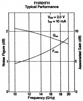
Fig. 3: Noise and gain figures.
Tests of such h.e.m.t. devices in high in performance, low-noise, amplifiers for use in earth stations for 30GHz uplink/20GHz downlink satellite communications showed that gains of 33dB could be obtained. Residual noise was reduced to 1.71dB (about half of that of conventional amplifiers using m.e.s.f.e.t. devices). Fujitsu plans to produce h.e.m.t.s for amplifying signals at frequencies of up to 50GHz.
An H503 h.e.m.t. from Gould is designed for a maximum operating frequency of 18GHz. This device is fabricated with a 0.5pm gate length by a m.b.e. process. The H503 is intended for satellite communications, radar and electronic warfare applications.
Sony, another Japanese company, produces 200µm wide 2SK676 and 300µm wide 2SK677 aluminium gallium arsenide on gallium arsenide h.e.m.t. devices (also known as h.i.f.e.t.s) by metal organic chemical vapour deposition (m.o.c.v.d.). Each device is available in three grades, with maximum noise figures of 0.1dB, 1.2dB and 1.4dB at 12GHz. Sony claims these devices are optimal for a wide range of front-end amplifier applications, including satellite reception and other communications systems from C band to Ka band and above.
Sony claims that the m.o.c.v.d. processing instead of normal liquid phase epitaxy (l.p.e.) or m.b.e. is the main factor in achieving ultra-low noise performance; it allows thin semiconductor layers to be built up with very precise thickness. The gate, the source and the drain are added later by conventional photolithographical techniques.
Sony's h.i.f.e.t.s are aimed not only at commercial applications such as 4 and 12GHz satellite signal reception, but also at communications and other applications at Ka band and above. The two models are available in both chip and packaged form.
The Californian Eastern Laboratories of the Nippon Electron Co. (NEC) offers an NE202 h.e.m.t. with a typical noise figure of 1dB at 12GHz with an associated gain of 12dB. At 2GHz the device offers a 0.3dB noise figure and 20.5dB gain, but h.e.m.t.s are usually too costly for use at 2GHz. Very high reliability can be difficult to obtain in new devices, but a protective passivation layer of silicon nitride is applied to each NE202 i.c. to avoid contamination. This device is more or less interchangeable with standard m.e.s.f.e.t. products, offering an immediate improvement in the noise figure and gain performance.
The very low noise h.e.m.t. produced by TRW Electronic System Group of California uses a 0.2µm T-shaped gate. A noise figure of 0.61dB at 12GHz has been measured with an associated gain of 12.58dB. This is claimed to be the lowest noise figure ever reported for a h.e.m.t. at this frequency.
T-gate Process
TRW reduced the noise figure in three ways. The T-gate process they developed increases the cross-sectional gate area and reduces the gate resistance.
A deep alloying technique is employed to reduce the ohmic and source resistance. The gate length has been reduced from 0.25µm to 0.2µm to minimise the gate-source capacitance and increase the transconductance.
The US General Electric Company of Syracuse, New York, developed a h.e.m.t. for millimetre wave allocation in phased array radars and satellite communications. It has a noise figure of 2.1dB at 40GHz with an associated gain of 7.0dB; these figures were said to be better than the best available m.e.s.f.e.t. at 40GHz at the time. A maximum available gain of 5.7dB was measured at 60GHz for this device whose cut-off frequency is about 80GHz. A noise figure of only 0.05dB was found at 3.3GHz in a cooled device.
The General Electric Company in collaboration with the University of Illinois has developed a gallium arsenide h.e.m.t. with a calculated clock speed of 230GHz. At present there is no equipment available which is fast enough to check the switching speed of the device. The 230GHz maximum frequency of operation, (where the gain is unity), was determined by extrapolating the measured gain at 60GHz (11.5dB), assuming the normal 6dB/octave roll off.
This device was developed for the Jet Propulsion Laboratory (JPL), Pasadena, California for use in radio telescope detectors, where extremely low noise figures are required to discriminate between very low-level space signals and background noise. This h.e.m.t. can replace the much bulkier extremely expensive maser amplifiers for signal detection.
The device was fabricated by depositing indium gallium arsenide on a gallium arsenide surface. The indium gallium arsenide forms the two dimensional electron gas channel instead of gallium arsenide. The indium gallium arsenide layer is unnaturally compressed, leading to the name pseudomorphic h.e.m.t. for this type of device. The gate length is 0.25µm. Such devices have produced gains of 11.7dB at 60GHz and 6.7dB at 94GHz. Applications for extremely fast signal processing are expected.
Integration
The very high performance of discrete h.e.m.t. devices will eventually be incorporated into economical microwave modules, hybrid devices and monolithic microwave integrated circuits (m.m.i.c.$). As long ago as 1983, Fujitsu announced the integration of a few h.e.m.t.s into a single device and in early 1984 produced a 4K static RAM with access times only a small fraction of those of other gallium arsenide or silicon devices. In January 1986, a 256 bit Fujitsu h.e.m.t. memory containing 2072 h.e.m.t. devices became the first digital h.e.m.t. i.c. to be marketed; it is designed for operation at - 196°C, but has a 1.5ns access time. In 1985 this manufacturer announced that a four-stage 19GHz h.e.m.t. amplifier was operating at liquid nitrogen temperature in a Japanese satellite as part of a communications link.
The Japanese have had a national plan which aimed to produce a scientific super-computer based on h.e.m.t. devices by 1989. It was predicted that it would out-perform even the projected Cray computers.
Monolithic Microwave i.c. (m.m.i.c.) devices using h.e.m.t.s are still in the laboratory stage, but progress is currently being reported on such devices as traveling wave m.m.i.c. amplifiers, especially for military applications. Workers at Varian in Santa Clara, USA report an improvement in microwave amplifier noise figures of about IdB when h.e.m.t.s are used instead of m.e.s.f.e.t.s in m.m.i.c.s for the upper microwave frequency range of 12 to 20GHz with smaller improvements down to 2GHz. The greater gain available from h.e.m.t. devices also contributes to the overall performance of these m.m.i.c.s.
It has been suggested that the availability of the h.e.m.t. with switching times of less than 10 picoseconds has been largely responsible for the winding down of intensive research on superconducting computers using Josephson junctions. HEMT switching speeds at the temperature of liquid nitrogen can be greater than that of Josephson superconducting junctions at liquid helium temperatures. However, the new high temperature superconducting materials may eventually change this position.
Conclusion
The availability of h.e.m.t.s has enabled a comparable performance to be obtained at millimetre wavelengths to that previously obtainable at much lower GHz frequencies. Although Japanese and a few US companies have been prominent in the h.e.m.t. market, it seems the number of manufacturers of these specialised products will be quite small unless the market takes off in some unexpected way.
Only large companies, with extensive research facilities, and advanced semiconductor processing equipment can sensibly enter h.e.m.t. manufacture. The h.e.m.t. manufacturing technology can also be employed for creating lasers on an i.c. High frequency quantum-well devices which depend on tunnelling through thin barriers are expected to provide a challenge to the h.e.m.t.
Integration of HEMTS
HEMT devices are attractive for integration into m.m.i.c. devices (monolithic microwave i.c.s), since the resulting m.m.i.c.s may have reduced i.c. size, improved receiver performance and an extended frequency of operation even into the mm wave region. It has been estimated that the advance of h.e.m.t. integration into operational systems is increasing by a factor of four each year. A number of monolithic circuits incorporating h.e.m.t. devices have been developed in the past few years which provide excellent gain and noise figure performance (see Table 1).
HEMTs are being used in military equipment (both hybrid and monolithic products). They are very suitable for electronic warfare application in the 2 to 40GHz frequency range, for phased array X-band radar applications, for 35GHz smart munitions, and also for the US Milstar military satellite programme using a 20.7GHz downlink and a 44.5GHz uplink with a 60GHz satellite cross-link band.
There is intense interest in the development of more advanced m.m.i.c.s utilising h.e.m.t. devices. Improvement in the materials and in the process technologies (leading to shorter gate lengths and mushroom gate profiles) are resulting in work on the development of monolithic h.e.m.t. low noise amplifiers for frequencies up to 100GHz. Various manufacturers are also developing power i.c.s using h.e.m.t.s for the mm wave region of the spectrum; advanced material structures such as a pulse-doped h.e.m.t. device or multi-channelled h.e.m.t.s can be used in such products.
Digital applications are expected to greatly intensify the importance of h.e.m.t.s during the 1990s. Details of the first digital h.e.m.t. i.c. became available in January 1986 when Fujitsu released details of its 256-bit h.e.m.t. memory. It includes 2072 h.e.m.t. devices and provides an access time of 1.5nano seconds at -196°C. The same company developed the fastest 1 Kbit static RAM with an access time of 0.9nanosecond at -196°C (1.5 times faster than any silicon i.c. on the market).
It has been forecast that h.e.m.t. technology will gain most attraction from large digital systems, such as mainframes and supercomputer manufacturers. Another area for development is that of telecommunications where h.e.m.t.s may play a very important role in the future. The technology used for h.e.m.t. fabrication can be used to create lasers on the same i.c. Instead of installing more optical filters in fibre optic systems, lasers emitting different wavelengths could be fabricated on i.c.s to increase the number of circuits which can be carried by a fibre optic pair.
| Manufacturer | Frequency (GHz) | Noise Figure (dB) | Gain (dB) | IC Area (mm) |
|---|---|---|---|---|
| Gen. Electric | 7.5 - 12 | 2.4 | 12 - 18 | 1.7 x 2.54 |
| Thomsom-CSF | 9.5 | - | 5 | 0.85 x 1.8 |
| TRW | 43 - 45 | 5 | 5.5 | 1.25 x 1 |
| Varian | 2 - 21 | 3 | 12 | 2.3 x 1.7 |
| Varian | 20 - 40 | 5 | 6 | 2.2 x 1.1 |
| Varian | 3-40 | 4 | 6 | 2.4 x 0.9 |
| Varian | 23 - 25 | - | 10 | 2.0 x 1.1 |