A valved transmitter for 3.5 MHz
Richard Q. Marris G2BZQ describes a simple valved 3.5MHz transmitter which is capable of good stability and is simple to make.
My transmitter project is a highly efficient, rugged and simple, low power c.w. unit delivering more than 10W. As it's crystal controlled with stabilised h.t., and a buffer stage between the crystal oscillator and power amplifier stages, it produces an exceptionally clean c.w. performance.
Valves are used throughout, as I think they are the most reliable. They're also easily replaced and readily available.
Every item used was found in my junk box. Many long forgotten bits and pieces were located in various parts of the QTH and garage.
The transmitter was designed around available components. It was fun building the transmitter and a pleasure to use it on air.
Many amateurs will have some, if not all, of the necessary parts. However, some components are readily available from advertisers of surplus or new components, and other sources such as rallies.
Simple Circuit
The project uses a simple circuit as the transmitter uses valves. All the valves used are readily available, and can be overrun and abused - unlike many transistors!
If the valves fail, you just pull them out and plug in a replacement. Remember that valves which were designed before the Second World War are still in use, so they must be considered reliable and worthy of use.
My prototype transmitter was assembled in to two units of approximately equal size. These are in the form of the transmitter and a.c. power supply.
The two separate units are interconnected with a cable and plug socket assembly. This is done so that the power supply unit (p.s.u.) can be used with other equipment.
However, the circuits and layouts I'm describing can be amalgamated into one chassis/cabinet to provide a complete transmitter with integral power unit. The dimensions are not critical.
Practically speaking, any suitable chassis/cabinet(s) can be used for the project. No real attempt at miniaturisation was made. The object was reliability, making it easy to build and easy to service.
Transmitter Described
The transmitter can be described as a 10 to 15W input unit. But my prototype seems quite happy running with 16W input (c.w.).
Conventional, well tried and tested circuitry has been used throughout. Signal strength with stability, quality and reliability was my target. The good quality of the resulting c.w. signal has been remarked on by other stations during QSOs.
The circuits are shown in Figs.1 and 2. Each circuit terminates with four power points, which have to be joined together.
The joining can be done with a cable/plug/socket arrangement. The sockets must be at the rear of the a.c./p.u. with the plugs from the transmitter.
Any a.c. existing p.s.u. providing 250-300V d.c. at 100mA, plus a 150V stabilised supply would be suitable. Two 6.3V heater windings of at 15 amp minimum are required.
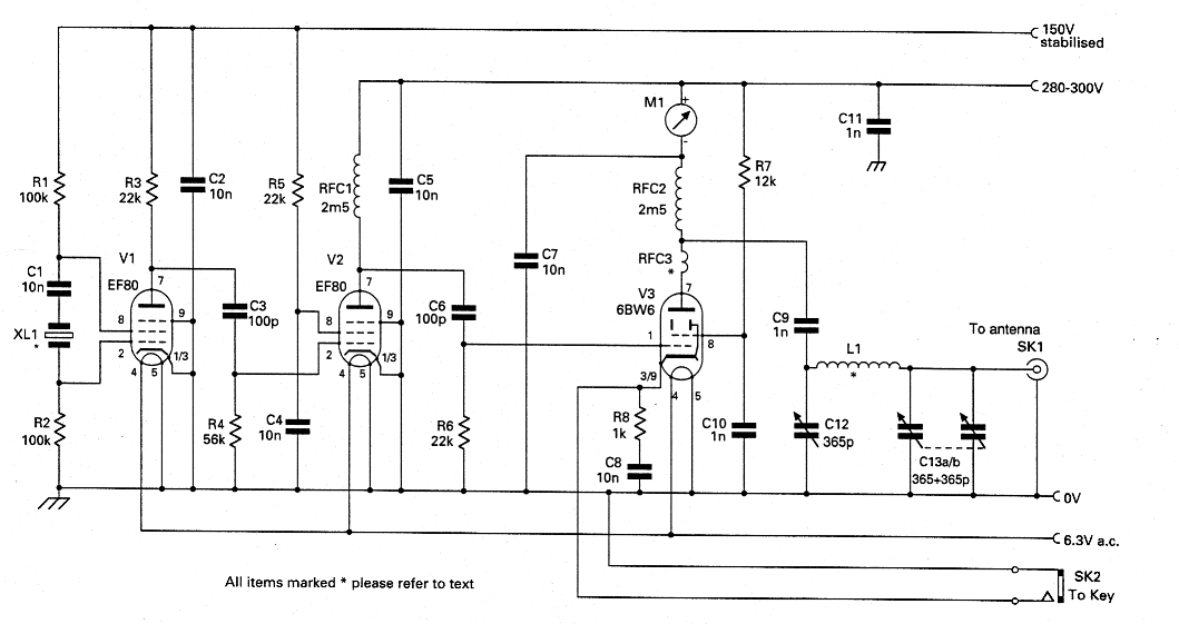
Fig. 1: Circuit of the 3.5MHz valved transmitter project described by G2BZa.
Crystal Oscillator
The transmitter line up, Fig.1, consists of a crystal oscillator stage, a buffer amplifier and a p.a. output stage. The suggested power unit, Fig. 2, consists of a valve full wave rectifier and a voltage stabiliser.
The crystal oscillator stage uses an EF80/6BX6 valve (V1) in a simple Pierce Colpitts crystal oscillator. This particular layout using g2 of the valve, V1, as an anode is called an electron coupled oscillator. The oscillator output is buffered by the anode circuit of V1.
The crystal socket (I used FT243 crystals) is mounted on the front panel of the transmitter unit. The oscillator is fed with stabilised hi supply (150V). There is a bit of luxury with a crystal type oscillator, but this technique ensures you ofvery clean and stable signals.
The next stage is the buffer amplifier with another EF80/6BX6 valve (V2). This is an extra stability refinement, giving some extra drive to the p.a. stage.
The power amplifier uses a 6BW6 valve (V3) which is rated at 11 to 12W input according to an old ARRL Handbook I have. The 6BW6 is supplied with 280V h.t. positive on the prototype, and uses a well tried and proven circuit.
A conventional network output tuned circuit is used to match 750 coaxial feedlines to a suitable antenna via a suitable matching unit. V1, V2 and V3 use B9A valve bases.
Editorial note: We strongly recommend, that to reduce possible EMC problems, that this transmitter be used in conjunction with a low pass filter unit. It should be connected between the output and the antenna tuning unit The filter should have a sharp cut-off above 30MHz.
Keyed Cathode
The p.a. stage is keyed on the cathode. To assist the prevention of interference, it's provided with suitable key click suppression.
A 100mA meter is wired into the anode circuit for tuning and loading purposes, and monitoring the anode h.t. current. By measuring the h.t. voltage on the anode circuit, and multiplying it by the anode current reading on the meter, you'll have the p.a. power input in watts.
The a.c. power unit I used provides 280V h.t., plus a stabilised voltage of 150 d.c. for the crystal oscillator. It consists of a mains transformer in a full-wave rectifying circuit using an EZ81/6CA4 rectifier valve (B9A base).
The two l.t. windings for the valve heaters should be 6.3V a.c. each. A minimum of 1 and 1.5A ratings respectively is required.
The h.t. is smoothed by means of a 10H 100mA choke. The choke works in conjunction with two 16µF electrolytic capacitors (min 450V working).
The 0A2 voltage stabiliser (B7G base) valve is used to provide the 150V h.t. line. A small 6V dial light bulb is wired into the heater circuit, and panel mounted to show when the power unit is switched on.
The switch, S2, is the StandbylTransmit (and net) switch. When the switch is `open' the h.t. to the transmitter is disconnected. When S2 is closed (with the Morse key up) only the crystal oscillator is running.
Holding the Morse key down brings the p.a. into action. Before testing, make certain that your receiver is suitably protected before you operate the p.a. stage.
In practice, S2 can be a pair of contacts on a send/receive relay (or switch). This can change over the antenna from transmit to receive.
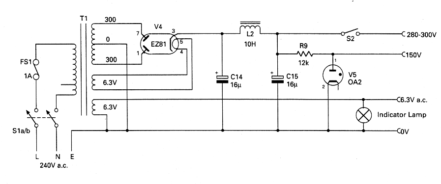
Fig. 2: A full wave rectifier power supply circuit, suitable for use with the 3.5MHz transmitter (see text).
Potenentially Lethal
Whatever switching arrangements are used on the transmitter, remember the voltages are potentially lethal. This is because there is approximately 300V on the switch contacts.
In operation, the receiver being used must be protected against the full `blast' of r.f. from the transmitter. Don't forget also, that r.f. voltages like mains voltages can be lethal. In addition, they must be treated with extra respect, as they can give you unpleasant r.f. bums.
My prototype transmitter was built into a small metal case, and another was used for the p.s.u. However, you might like to build the unit into one case.
The layout of the main components is not critical, and the exact position of the componentswill vary depending on the size of the actual components used. However, it's best to follow good r.f. practice and screen the transmitter to reduce EMC problems.
All resistors are 0.5W watt rating except where otherwise indicated. Capacitors are 350V working (minimum) unless otherwise stated.
Good quality capacitors should be used in this project. Decoupling capacitors should be connected as close as possible to their points to be decoupled. They should be grounded directly to the nearest point of the chassis, and securely fixed with solder tags.
Tuning Inductance
The main p.a. tuning inductance is wound on a 1in diameter Paxolin tubing. I wound 35 turns of 24s.w.g. enamelled copper wire on the tubing, with spacing of a wire diameter between turns.
A simple anti-parasitic choke is provided by RFC3. It consists of seven turns of pvc covered single core hook-up wire, wound onto a 0.125in diameter rod as a mandrel which is then removed. The result is a self-supporting choke.
All wiring should have adequate insulation and be carefully soldered. This precaution is essential when you're dealing with a.c. mains and h.t. voltages. The switches S1 and S2 should be good quality switched operating well within their voltage ratings.
Testing Stage
After you've carried out the usual safety checks (for shorts and wiring errors), you cati start the testing stage. With the power supply connected, a 3.5MHz band FT243 crystal (or other suitable type) is plugged into the crystal socket mounted on the front panel.
Next, you should connect a 15W (minimum) dummy load (5052 impedance) into the antenna socket. You are now ready to switch on.
To start, S2 is put into standby position (contacts open). On switching on the power unit switch, S1, to on, the dial light should come on and there will be no reading on the meter. The `off load' h.t. voltages should be checked after allowing two minutes warming up period.
Now switch on S2 and with the Morse key up, there should still be no meter reading. But it should be possible to pick up the crystal oscillator on a nearby receiver - tuned to the crystal frequency of course.
With both variable capacitors at minimum capacity, S2 is closed to apply h.t. to the p.a. stage. Holding the Morse key down will produce a meter reading, and C12 should be quickly rotated for the minimum current dip on the meter - this is resonance.
The other variable capacitor, C13a,b, should be increased until a reading of about 40mA appears on the meter. Now retune C12, for minimum dip, and if necessary, increase again back to 40mA.
On the prototype, with antenna connected, I found the transmitter can be loaded to 60mA at 280V h.t. This corresponds to 16.8W input, and the 6BW6 valve seems to be quite happy about this level.
The stability and c.w. note canbe key checked with the receiver, with the r.f. gain turned well down and the transmitter operating into a dummy load or antenna.On The Air
On the air the c.w note should be found to be absolutely clean, sharp, with no chirp. This is entirely due to the use of a crystal oscillator with stabilised h.t., and a buffer amplifier between the crystal oscillator and p.a. stages. To get the best out of this approach, the transmitter must use rigid construction techniques.
Initial loading in the antenna is identical to that of the dummy load. However, if the antenna impedance is very low, it may be necessary to connect a high voltage ceramic disc or silver mica capacitor (1kV working) across C12a,b.
In practice I found that capacities of 500 or 750pF should suffice. Such a situation might arise with an end fed wire, but in practice a good a.t.u. and low pass filter should always be used with any antenna.
The circuitry of the transmitter is a little above average for a valved rig. But the refinements used, are well worth while for anyone wishing to put out a T9++ c.w. signal on 3.5MHz.
Good luck with your junk box transmitter. It's cheap to make and should provide a lot of enjoyment on the air.