Plate characteristics of a distortion-free class-AB RF amplifier Tube
An ideal tube, free from odd-order distortion, provides a unique basis for discussing source-impedance issues. Lets look at what happens at its plate over a full cycle of RF.
Over 40 years ago, I published a tube transfer curve(1), (2), (3) that would provide distortion-free operation of a class-AB power amplifier. The object was to provide tube manufacturers with a goal for new tube designs.
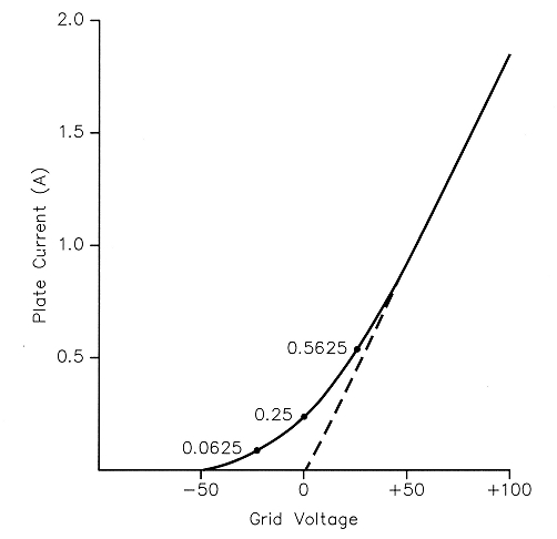
Fig 1 - Distortion-free transfer curve.
The curve is shown in Fig 1. It consists of two parts. The curved part is a square-law curve that starts at the point of plate-current cutoff and rises as the square of de grid voltage. The second part continues from the end of the square-law curve at the same slope in a straight line. A representative length of the straight part is shown. A longer straight part gives lower idling current and better efficiency. The de bias voltage must be located exactly halfway between the ends of the square-law curve, as illustrated. An extension of the straight-line part of the curve will pass through this bias point, which is 0 V in the illustration. When a small sine-wave voltage eg is applied to the grid (after dc bias and plate voltages), the plate current remains on the square-law part of the curve. It conducts over the entire RF cycle, which is a definition of class-A operation., The plate current consists of a de component, a fundamental or linear component and a small secondharmonic component. There are no odd-order components, such as third, fifth, seventh and so forth. Therefore, there will be no odd-order IMD when multiple tones are applied.
When the grid signal extends beyond the square-law curve, it simultaneously extends into the straight-line part of the curve and into the plate-current cutoff part (which is also linear). Thus, there are no odd-order harmonics or IMD products produced when operating up to the end of the straight-line part of the curve. There are even-order products, such as the second, fourth, sixth and so forth, but these are removed by the tube's plate tank circuit. Thus, we have an IMD-free tube transfer curve for class-AB operation.
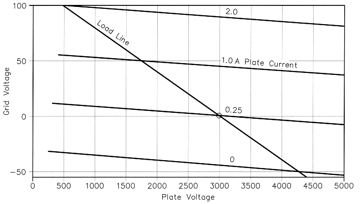
Fig 2 - Distortion-free constant-current curves.
Fig 2 shows a set of hypothetical tube-constant-current curves that incorporate the above distortion-free properties. The lowest line represents plate-current cutoff. The next line represents the value of idling plate current required for distortion-free operation at a given plate voltage. The third line represents the current at the junction of the square-law and the straightline curves. The fourth line represents the end of the straight line, beyond which the grid should not be driven. It is arbitrarily located at twice the current at the top end of the square-law curve. The end of the tube load line for maximum power with no distortion is located at the end of the linear-current range (for maximum plate swing) and the maximum value of peak plate current that keeps the maximum average-de plate current within the manufacturer's limit. A lower value may be selected to keep the tube's operation within its maximum-plate-dissipation rating, or to operate at some lower PEP outputlevel.
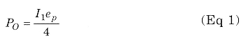
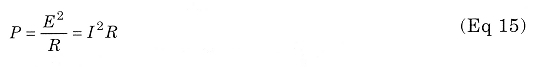
The power output is computed from I1, the peak fundamental value of plate current, and ep, the peak platevoltage swing, using the relation:
The values of I, and PO are exactly the same as if the tube were operated in pure class-B with 180° of plate-current flow and extremely sharp cutoff (no square-law part of the curve). In Fig 2, the plate-current cutoff line would be located where the dc-bias line is located. The current spacing between all the lines would then be the same. In Fig 1, note that if the plate current below the dc-bias voltage is folded over to the right and subtracted from the upper portion of the square-law curve, we are left with the straight line of a theoretical class-B transfer curve. The de idling current for pure class-B operation is zero.
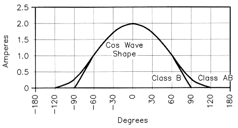
Fig 3 - Superimposed pure class-B and class-AB plate-current pulses.
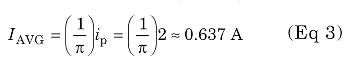
Fig 3 illustrates the shape of class-AB and pure class-B plate-current pulses superimposed one upon the other. The pure class-B pulse is a half sine wave. In this example, the peak value of the fundamental component of the half sine wave is:
The average plate current of the half sine wave is:
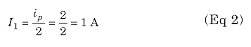
The current for class-AB is a little higher because of the added current in the cutoff region (the square-law part of the curve). The area outside of one of the half-wave cutoff points, which conducts over 1/12 of the RF cycle is:
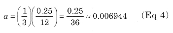
There are four such conduction periods: two inside and two outside the half-wave cutoff points. Therefore, the total dc plate current is:
![]()
which is an increase of only 0.0277 A, or 4.35%, above the pure class-B value. This added current at maximum PEP output is much less than the idling current of 0.25 A. This is why high idling current doesn't increase the plate dissipation loss very much at full, single-tone PEP output.
In Fig 2, the dc plate voltage is 3000 V and peak plate swing is 2500 V. The power input and output are:
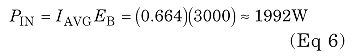
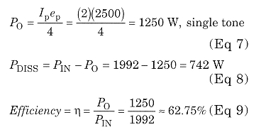
For comparison, the plate efficiency for the theoretical pure class-B case would be:
at 1250 W single-tone output. The RF plate load resistance is:
at the fundamental. The idling or zerosignal plate dissipation for class AB is:
![]()
Computing Plate Resistance Rp and Output Source Resistance RS from Tube Curves
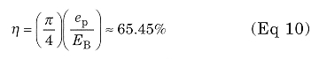
Rp is determined by:
at a constant grid voltage at each location on the tube chart. The current increases linearly with grid voltage above the 1 A constant-current line on the chart. Therefore, Rp is constant for all points on the chart above that line. Its value is:
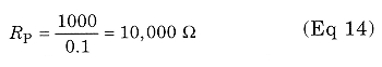
at all points above the 1 A constantcurrentline.
Rp increases as the point in question is moved downward from the 1 A constant-current line and reaches infinity at the 0 A constant-current line. Note that the AI becomes smaller for any given AE as the chosen point is lowered, which causes the rise in Rp. Fig 4 shows a plot of the reciprocal of Rp, which is conductance Gp, plotted against grid voltage. This plots as a straight line centered on the de bias voltage.
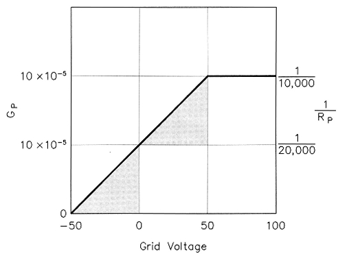
Fig 4 - Plate conductance 1/Rp versus grid voltage.
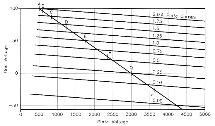
Fig 5 - Distortion-free constant-current curves with more current lines and a load line with points marked for Chaffee analysis.
Computing Rp and RS from a Chart of Tube Constant-Current Curves
Fig 5 is the same as Fig 2, but with a few more plate-current lines added to better represent typical tube curves published by manufacturers. In Fig 4, note that Gp at the bias voltage (on the 0.25-A line) is exactly one-half of the Gp in the linear region above 1 A. This means that Rp at the bias or zero-signal point is exactly twice the value in the linear region. Thus, Rp is (2)(10,000) = 20,000 ~2 at this point.
Consider a very small RF signal voltage, such as 1 V. The value of Rp is nearly constant over the entire cycle. Therefore, RS is 20,000 Ω. When the RF grid-voltage swing extends beyond the region of the square-law curve (beyond 0-1 A), the value of Rp is infinite when the grid voltage is below cutoff and remains fixed at 10,000 Ω for values that produce more than 1 A of plate current. Since the time in the cutoff region is equal to the time in the constant-Rp (10,000 Ω) region, the average value of Rp in this case will be 10,000/0.5 = 20,000 Ω. This is the same as the value in the low RF grid-voltage region. Therefore RS, which is Rp when averaged over a complete RF cycle, is the same at all values of RF grid-voltage swing (within the maximum plate-voltage swing and peak-current limits). Therefore, we can conclude that RS 2Rp for this ideal class-AB tube.
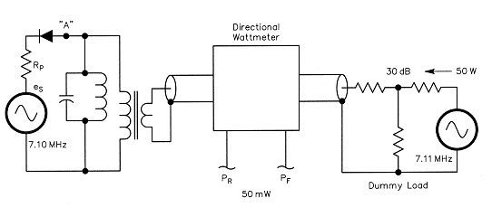
Fig 6 - Functional equivalent Bruene test circuit (see Note 4) when transmitter signal is present, up to full power for pure class-B operation.
Now let us address how to determine the value of RS by computation data obtained from the tube curves. First, consider the case of pure class-B operation for which Fig 6 is valid because Rp is constant over the conduction period of the "diode". The Chaffee-analysis concept is used to compute the fundamental component of the test-signal power flowing in Rp. A plate-current data point is taken at the peak of e and at each 15° interval; those are labeled points A, B, C, D, E, F and Q. The current value at Q is zero, and for pure class-B, all values beyond Q are also zero. The power delivered to the resonant circuit is the sum of the powers delivered over each 15° interval. It varies over the half wave as the square of the signal amplitude (in this theoretical class-B tube), since:
Thus, we must weight each current sample according to the square of the voltage amplitude of each sample. Note: I have chosen to integrate over only 900 and double the result, since the other half is the same for a resistive load. Point A is divided by two, since there is only 7.5° in one-quarter cycle. The other points are weighted according to the square of the voltage amplitude, which is Bcos2Φ, Ccos2Φ, and so forth:
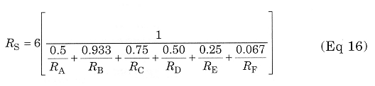
All those resistance values are 10,000 Ω for the hypothetical class-B case. RS is 20,000 Ω, which is 2Rp; but the same as we previously determined for the small-signal class-AB case, which is equivalent to class A. The complete equation for computing RS for class-AB operation is:
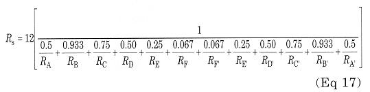
Note: Eq 17 may be changed to use plate conductances by multiplying the weighting factors by the conductances instead of dividing by the resistances. A computer program was written to compute RS for various RF peak grid-voltage levels from 10 to 100 V for the transfer curve shown in Fig 1. It was found again that RS is 2Rp for all signal levels.
Eq 17 can be used to compute RS for a selected operating condition of a real tube. The values of Rp, or Gp, must be determined from the tube constant-current curves for data points A, B, C etc.
The effect upon RS of driving the tube into the nonlinear region can be computed. Rp at points A and B can become very low. Since these points are weighted most heavily in Eq 17, the value of RS may drop dramatically. With sufficient overdrive, RS can be reduced to the value of RL and even lower. But that is beyond the linear range of the tube and should never be reached in SSB operation.
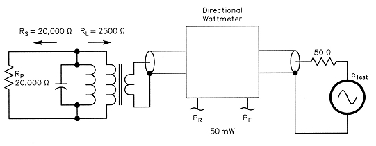
Fig 7 - Equivalent Bruene circuit (see Note 4) for measuring Rs with the RF amplifier on, but no drive present.
Measuring RS
Fig 7 shows the essential functions of my method4 of measuring RS with a very small test signal when the power amplifier is on, but with no drive applied. The Rp of our theoretical tube is 20,000 Ω, which is also RS for a small test signal. The parallel-resonant circuit represents the selectivity of the RF output network (or tank circuit). An ideal transformer transforms the 50 Ω load impedance up to the RL of 2500 Ω plate load resistance. A length of coax produces the same phase delay as the output network. The bidirectional wattmeter measures the forward power of the test signal going into the power amplifier and the reflected power returning from the power amplifier. The test signal has a source resistance of 50 Ω. When we apply the test signal, producing 50 mW of forward power, we find a reflected power of 30.247 mW (assuming a loss-less output network). From that, we compute an SWR of 8:1. This is correct because the 20,000 Ω RS is the actual load (at the test-signal frequency) across the tuned circuit; but looking toward the test generator, the source impedance is equal to the RL of 2500 Ω.
In actual practice, using a linear with a typical output network, the reflected power will be less by perhaps 20% or more because the signal has to pass through the output network twice. Estimating the output network's loss and increasing the measured reflected power by this amount is necessary for an accurate determination.
Fig 6 illustrates the functions when the RF amplifier is operating in pure class B. The Thevenin-equivalent-circuit concept is used to represent the power-amplifier tube operating into a tuned output network. The tube conducts for exactly 180° and therefore acts as a diode. The tube may be operated at any power level up to the limit of its linear range. The theoretical voltage eg, is that required to develop the necessary RF plate voltage across RL at the input to the resonant circuit. The frequency of eg is the frequency being amplified by the power amplifier, which will be 7.10 MHz in this example. The test signal is now fed into the coax through a 30-dB directional coupler, which directs 50 mW toward the power amplifier and the rest of the 50 W test signal to a 50 Ω dummy load. This load is also the load for the amplifier under test. The test frequency is typically separated 10 kHz from the main-signal frequency, making it 7.11 MHz in this example. It must be close enough so the resonant circuit will pass both frequencies, but far enough away so that the test instrument can measure the two voltages separately. A good spectrum analyzer has enough selectivity to do this. The 50-mW test signal travels toward the tube much as an ordinary reflected wave of the main signal would (if present).
The plate resistance is 10,000 Ω in the conduction region, so the current flows in half sine-wave pulses, which contain the fundamental, dc and harmonic components. The tuned circuit bypasses the dc and harmonic components to ground; therefore, the test circuit only measures the fundamental component of the current in the half sine-wave pulses. The peak value of the fundamental component is one-half of the peak amplitude of the half sinewave current pulse.
Now let us apply eg, with amplitude that would produce full power (1250 W) into the plate load resistance (2500 Ω). The voltage across the resonant circuit is 2500 V peak. Current flows through es in half sine-wave pulses. The fundamental component of is, is 1 A peak. The peak current in the half sin wave is twice the peak amplitude of the fundamental component; therefore, it is 2 A peak. The peak voltage of es (which doesn't actually exist) is:

The average current is:

which is the dc value.
At point "A" (representing the tube anode), the test signal is traveling from the right and "sees" Rs. If RS is higher or lower than RL, part of it the test signal will be reflected and travel back toward the dummy load. Its magnitude can be read on a spectrum analyzer connected to the directional coupler. The SWR can be computed from forward and reflected power samples at the test frequency.
The RF voltage across the resonant circuit consists of the phasor sum of the 2500 V signal voltage (at 7.10 MHz) and the sum of forward and reflected components of the test signal (at 7.11 MHz). The wave shape of the phasor sum voltage at A is very close to a pure sine wave over any one cycle. It takes 10,000 cycles of the small 7.11 MHz phasor to make one revolution around the end of the 7.10 MHz phasor. Thus, the change from one RF cycle to the next of the sum is very small. The "diode" rectifies the composite voltage wave, which is tantamount to rectifying both components.
Conclusion
A hypothetical distortion-free tube for class-AB operation has been found a useful analytical tool. Also, it provides: tube manufacturers with a goal for tube design and RF power-amplifier designers with an understanding of how to choose an optimum operating condition.
Notes:
- W Bruene, "Linear Power Amplifier Design", Proceedings of the IRE, Dec, 1956, pp 1754-1759.
- Pappenfus, Bruene, Shoenike, Single Sideband Principles and Circuits, (New York: McGraw Hill, 1964).
- Sabin, Shoenike, HF Radio Systems and Circuits (Norcross, Georgia: Noble Publishing, 1955), pp 546-547.
- W. Bruene, W50LY, "RF Power Amplifiers and the Conjugate Match", QST, Nov, 1991, pp 31-33, 35.
W5OLY