The transistor - or 25 miles on a hunk of Germanium
Some background on the tiny devices that may revolutionize the electronic art.
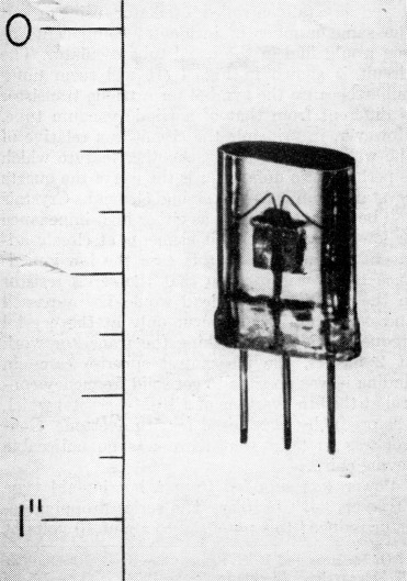
A point-contact transistor, three times actual size.
The first use of a transistor for transmitting purposes was reported in QST last month. Here the designer of the tiny rig that appeared on our February cover describes it in detail, and provides us with some basic information on transistors and their potential uses.
Most HAMS who can qualify for the Old Timers Club remember with mixed feelings the time spent per evening searching for that elusive spot on their pet piece of galena which would bring in NAA at a readable level, if not exactly loud and clear. Neither they nor anyone else knew why or how the thing worked in the first place. When tubes finally became commercially and financially available it was the general hope that galena and its sister crystals silicon, carborundum, etc., would be properly disposed of. They did practically vanish from the electronic scene until World War II when silicon diodes were found to outperform tubes as microwave mixers. However, in some of the research laboratories scientific interest in these so-called solid-state semiconducting materials was very much alive. The usefulness of crystal diodes in military equipment intensified this interest and gave rise to some extensive research programs.
A bit of transistor history
While engaged in semiconductor research at the Bell Telephone Laboratories, Messrs. Bardeen and Brattain(1) observed that if two cat whiskers were placed very near each other on a piece of germanium and current was made to flow between each cat whisker and the germanium, the two currents would react on each other. The remarkable thing was that a small change in current through one whisker would make a larger change in current through the other. This is amplification, and any electronic device which will amplify is of more than passing interest. Thus the transistor was born.
Further research showed that power amplifications of 100 times or more could be readily achieved. From this point it takes little imagination to visualize the usefulness of such a simple device; no hot cathode, very small size, and apparently nothing to wear out or get used up.
In the short space of five years the amount of scientific effort and the number of dollars spent on the transistor family has ballooned to millions of man-hours and of dollars. Even more fantastic is the fact that most of this investment is still in development rather than in production.(2) Both industry and the government are gambling on the future of the transistor, but it looks like the odds are all favorable.
The lowest-powered transmitter
Now what has all this to do with the average ham? Actually nothing very much at this time, except that being a person possessing more than average scientific curiosity and ability he likes to anticipate his next or next-after-next project.
The writer, being fortunately situated with respect to transistor availability, was able not only to anticipate but also to carry out a pet ham project of many months' standing. This was to generate r.f. power, no matter how small, on two meters and see if the resulting signal could be heard beyond the confines of the shack. The two-meter band was chosen for two reasons. First, K2AH has a decent antenna (12-element beam) on two meters. Second, transistors were not supposed to work at frequencies as high as 146 megacycles. Ordinary transistors do not, but we in RCA had managed to put together some special ones which oscillated not only at 146 Mc. but which continued to do so above 300 Mc.(3)
A bit of arithmetical juggling of decibels and the known outputs of several 2-meter rigs came forth with the answer that anything over about 10 microwatts in the 12-element beam would be "gravy" over a path 15-20 miles long. It worked out just that way. We were sure of 30-50 microwatts from the transistor transmitter, so it was with considerable confidence that we asked Tommy Thomas, W2UK, of New Brunswick, N. J., to listen for us at 146 megacycles. He promptly came back and reported the signal RST 559. Tommy is a bit over 25 miles away as the signal flies. We then had contacts with W2KNI, Mountainside, N. J., and with W2DPB in East Orange, N. J., both of whom are about 15 miles away. Our own QTH is Mountain Lakes, N. J.
The transistor transmitter itself was simply a keyed crystal-controlled oscillator using about the same number of incidental components as one would find in the usual tube oscillator. The circuit is shown in Fig. 1. It will seem unfamiliar because the symbol for a triode transistor is different from that of a triode vacuum tube. However, in principle the circuit is a relative of the well-known Colpitts. Another feature which is perhaps also unfamiliar is the use of the quartz crystal as an r.f. by-passing element. Crystals can be made to operate as either high-impedance or low-impedance circuit elements at closely adjacent frequencies. In this case the low-impedance mode was used so that the series resistor in the transistor base lead would be by-passed and oscillation would occur only at the crystal frequency. Next to making the transistor work at 2 meters, the pleasantest surprise came in finding it was possible to get solid frequency control at the 9th overtone of a 16 Mc. crystal which was originally maximized for 5th overtone. Control was so tight that there was no noticeable keying chirp.
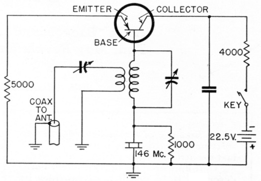
Fig. 1. Schematic diagram of the transistor crystal oscillator used on 146 Mc by K2A11. The only unfamiliar element is the symbol for the transistor itself. Values in the tuned circuits are dependent on the frequency used, but this general circuit works with crystals of much lower frequency as well.
Power was supplied from a hearing-aid type 22%-volt "B" battery. The series dropping resistor reduced this potential to about 10 volts at the transistor so that the total power to the oscillator was about 30 milliwatts.
We have not had the time at this writing to replace the series dropping resistor in the transistor collector circuit with a modulating transistor, but this is possible and will be done in time.
Even though Project Transistor QSO is in the category of hobby-horse riding, its accomplishment does serve to underscore the potential importance of transistors in the field of electronics. Somewhere in the first few paragraphs we used the term "transistor family," and did so deliberately because there are already several different members. Many more will certainly be forthcoming.
Types of transistors
The kind used in the 2-meter ham rig is a "point-contact" transistor in development by RCA consisting of two phosphor-bronze "cat whiskers" touching a small piece of germanium at points less than a thousandth of an inch apart. Germanium is a basic element and, like silicon, galena, and certain other materials, is in the class of semiconductors. These are peculiar materials in that they are neither good insulators nor good conductors.(4) They have another property which is both interesting and useful. Any metallic contact which is made to them with fairly light pressure will be found to carry current more easily in one direction than in the other, and is thus rectifying. There is as yet no good explanation but the effect seems to be a combination of electrochemical and mechanical action which disturbs the atoms of the semiconductor in the region of the contact. Well-soldered contacts do not exhibit this rectifying effect. This "disturbed" region of the semiconductor is called a "barrier" and can be thought of as a swinging door having a stiff spring on one side and a light spring on the other.
The point-contact transistor then consists of two of these rectifying contacts closely adjacent to each other on a piece of germanium. Typical construction is shown in Fig. 2. Of all the various semiconducting materials explored so far germanium seems to work best, so most transistor development centers around its use.
One of these contacts, called the collector, is biased several volts (sometimes as high as 30 or 40 V) in the direction of poor conduction, so that only a small amount of current flows. Figuratively, we are trying to open the door against the stiff spring. The other contact, called the emitter, is biased a few tenths of a volt in its direction of good conduction. As this emitter bias is applied, the collector current will be observed to increase substantially and will increase 2 or 3 times as rapidly as the emitter current increases. The emitter current, therefore, reduces the effectiveness of the "barrier" at the collector contact, or in effect reduces the stiffness of the stiff spring in our door analogy. We, in effect, get a "current gain" of at least 2 or 3 times. This in itself is not very impressive, but now let us measure two other electrical properties. The input or emitter circuit resistance is found to be about 500 ohms, and the output or collector circuit resistance about 20,000 ohms. A bit of arithmetic, using Ohm's law, shows we have a power amplification of about 100, which of course "ain't hay.
So much for the point-contact transistor, except to point out something you might have overlooked. The transistor is a current-controlled device in contrast with the vacuum tube which is a voltage-controlled device. This means that transistor circuitry will be different in many respects from the familiar tube circuitry. It also means that direct performance analogies between vacuum tubes and transistors can lead to considerable confusion and should be avoided.
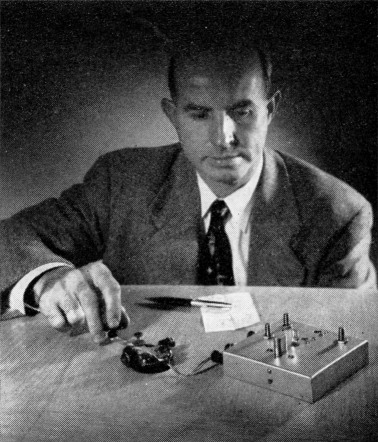
The author and his transistor rig.
These remarks apply almost equally well to another type of transistor which is receiving about the same amount of technical attention as the point-contact transistor. This one is known as the "junction" transistor. It appears to be even more promising than the point-contact type, particularly at low and medium frequencies. Power gains as high as 100,000 in a single stage have already been measured. Physically the junction transistor is quite unlike the point-contact type, as can be seen from Fig. 2, although there is some similarity in principle. It, too, has two "barriers" but these are located opposite each other on or within a piece of germanium crystal. One technique for creating these barriers, or junctions, is to diffuse another material, such as the metal indium, into two sides of a small slab of germanium. Electrical connections are made as shown in Fig. 2 to each of these junctions. The third contact in both types of transistor is a non-rectifying contact soldered to the body of the germanium piece and is called the "base."
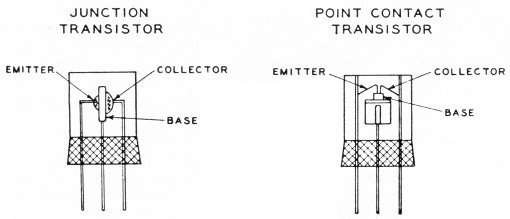
Fig. 2 - Basic details of junction and point-contact transistors.
The explanation for the occurrence of power amplification in the junction transistors is somewhat less complicated than is the case with the point-contact transistor, but is still too abstruse to attempt here except to again say that the two junction areas interact. A more thorough explanation calls for the use of the concept of conduction by "holes" in addition to conduction by electrons. Holes are places in the germanium crystal atomic structure where electrons could be but are not. Although this sounds ridiculous it has considerable foundation in fact. These holes do enter into the conduction process and behave as if they were positive electrons. There is no analogous effect in vacuum tubes.
It is quite possible to make transistors in which either electron or hole conduction is predominant. One can therefore make transistors which have almost identical electrical characteristics except that the applied battery potentials are exactly reversed in polarity. It would be just as if we could make positron tubes as well as electron tubes. This is particularly intriguing to circuit specialists because it makes certain types of circuitry possible with transistors which are either impractical or perhaps impossible with tubes.
They have shortcomings, too
Transistors in their present stage of development have many shortcomings such as temperature dependence, certain types of instability, excess noise, and power as well as frequency limitations. The encouraging thing, however, is the fact that no one has yet been able to prove that these defects cannot be overcome in time.
The main purpose of this article is not so much to explain transistors as it is to acquaint you with the fact that there is a new member of the electronics family which is already extremely important and about which you are certain to hear more and more. Unfortunately you will probably find it virtually impossible to lay hands on transistors suitable for v.h.f. experimentation. Be patient, because the day will certainly come when you can obtain them with ease.
Notes
- J. Bardeen and W. H. Brattain, "Physical principles involved in transistor action," Bell System Technical Journal, April, 1949.
- B. N. Slade, "Survey of transistor development," Radio & tv news, Sept., Oct., and Nov., 1952.
- G. M. Rose and B. N. Slade, "Transistors oscillate at 300 megacycles," Electronics, Nov., 1952.
- W. Schockley, "Electrons and holes in semiconductors," published by D. Van Nestrand Co., Inc., 1950,
George M. Rose, K2AH.