Diode modulators
Until the current interest in single-sideband transmitting techniques, amateurs had little or no contact with diodes used as modulators. While it is true that we have been using them for years as demodulators - "detectors" is the common word - there was never any reason to consider their use in the allied function of modulator. Their use as modulators is old hat to the commercials, however, particularly in the field of carrier telephony, and if you work for the telephone company you have probably run into them hundreds of times.
But before we get into a discussion of diodes, let's review some of our basic concepts and terminology, because it will help us to understand a few things later on. You are all familiar with the plot of an alternating current or voltage with respect to time. This is shown in Fig. 1A, where the time is represented along the horizontal axis and the amplitude is shown on the vertical. An alternating current or voltage of a single frequency is called a "sine " (or "cosine") wave, from the trigonometric function that defines the instantaneous values. It is symmetrical about the I zero-amplitude axis, the positive peaks extending as far above as the negative peaks do below. Along the time axis, the distance between similar parts of the wave is a time equal to 1/f, where f is the frequency. If the wave in Fig. lA is to represent a 1000 cycle wave, 1/f is 0.001 second, but if it were a 100 kc. wave, 1/f is 0.000 01 second. Drawn to the same scale, the 1000 cycle and 100 kc. waves might look as in Fig. 1B. But remember that the shape is always the same, and that only the scale changes. It's something like those trick mirrors in a penny arcade - they change the scale in one or the other dimension.
One very important thing to remember from the preceding paragraph is that a single-frequency a.c. wave is always symmetrical about the zero axis. If it isn't symmetrical, it isn't a single-frequency affair. Take, for example, the job shown in Fig. 10. At first glance it looks exactly the same as that in Fig. 1A, with the zero-amplitude axis displaced. (That's just what it is.) But it no longer represents a pure a.c. wave, because it doesn't satisfy our definition of being symmetrical about the zero-amplitude axis. Instead, it is now a representation of the a.c. wave of Fig. lA plus a d.c. (zero-frequency) component. It is obtained by adding the a.c. wave to a steady d.c. value, as shown. The polarity never goes negative, in contrast to the pure a.c. wave where the polarity is negative half the time. (Of course, the d.c. component could be negative, in which case the polarity would never go positive; or the d.c. component could be less than the peak value of the a.c., in which case the wave would fall on both sides of the zero-amplitude axis, but not symmetrically.)
This a.c. wave with a d.c. component is easy to come by, and exists in many places throughout radio equipment. The current in an audio amplifier is of this type, where the d.c. component is the steady value of plate current and the a.c. component is the audio signal. But there is one more thing we should know - and remember - about it. If the d.c.-plus-a.c. signal is coupled to anything, like a load or another stage, through a condenser or a transformer, only the a.c. component appears at the load. This should be obvious, of course - the condenser or transformer cannot pass the d.c., and anything passing through the condenser or transformer must swing equally about the zero-amplitude axis. Thus the signal of Fig. 1C passing through a condenser or transformer - or "a.c. coupler" -- will appear as Fig. 1A.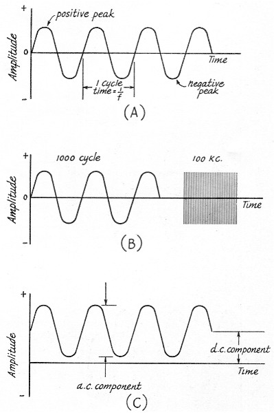
Fig. 1. The old sine wave, familiar to one and all, is shown at (A). It is a plot of amplitude vs. time of a single-frequency a.c. wave.
Two different frequencies drawn to the same time-base scale look entirely different, because the higher-frequency cycles are necessarily crowded (B). The shape is the same, however - only the scale is different.
A pure single-frequency a.c. wave must swing equally above and below the axis - if it doesn't, it has a "d.c. component" (C).
Envelopes
Before we settle down to the main business at hand, there is one more aspect of a.c. that we should review. The signals in Fig. 1 were drawn for only a few cycles, for convenience and ease of studying, but we should worry a little about how they start and stop. Suppose we examine a 100kc. signal that builds up slowly (instead of instantaneously as in Fig. 1B) and then decays slowly. It might look as in Fig. 2A. The first few (and the last few) cycles do not have the same peak-to-peak amplitude that the main bulk of the cycles do. The outline of the 100 kc. wave is represented by the dashed line and is called the "envelope." Notice particularly that this dashed line (envelope) does not represent the instantaneous value of the wave, but only the limits of its peak-to-peak excursions. It is, however, symmetrical about the axis, and must always be so if no d.c. component is present.
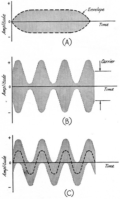
Fig. 2. High frequency waves don't start and stop instantaneously, and the outline of their rise and fall is called the "envelope" (A). Each cycle swings equally above and below the axis, however.
The familiar envelope of a "modulated" wave is shown at (B), with the less-familiar pattern of "superimposed" waves at (C).
Fig. 2B should be a familiar picture. It represents this 100 kc. signal we have been using "modulated" by our 1000 cycle signal. Actually, the only a.c. signal drawn here is the 100 kc "carrier," although we immediately recognize that the envelope has the form of our 1000 cycle signal. The amplitudes of the 100 kc cycles are changing from time to time. Notice also that, looking at the half r.f. cycles above the zero-amplitude axis, the outline bears a strong resemblance to Fig. 1C, except that in Fig. 2B the envelope replaces the signal, and the (half) carrier amplitude replaces the d.c. component. The same picture, flopped over, appears below the zero-amplitude axis, and the envelope is symmetrical about this axis, as it was in Fig. 2A. Remember that the only a.c. existing here has a frequency of 100 lie. (and some 99 and 101 kc side frequencies that we won't discuss), and that there is no 1000 cycle component that we could find with a wave analyzer.
But consider the signal in Fig. 2C. Here a 1000 cycle signal and a 100 kc signal exist in the same circuit. It is no longer symmetrical about the zero-amplitude axis. Instead, one signal is "superimposed" on the other, and a wave analyzer or tuned circuit could select one or the other quite easily. This is the basic difference between this "superimposed" wave and the "modulated" wave of Fig. 2B. In the superimposed waves, the peak-to-peak amplitude of each 100 kc. cycle is the same as that of the previous cycle, even though the excursion above and below the zero-amplitude axis is not always the same. And the envelope is not symmetrical about the zero-amplitude axis - it is as though the 1000 cycle signal had become the axis (dashed line).
Now that you can recognize the difference between superimposed signals and modulated signals, and know the effects of a.c. couplings, we are ready to talk about the mechanics of modulation in a diode.
Modulation
If we feed the superimposed signals of Fig. 2C into a resistor (or into a good Class A or Class B amplifier of such bandwidth as to pass 1000 cycles and 100 kc.), they will come out looking exactly the same as they did at the input. But suppose we use the circuit of Fig. 3A, and feed them into a diode? The action can be analyzed by plotting the effect in the diode, as in Fig. 3B. Whenever the 100-kc. applied voltage swings to the right (is positive), the diode conducts and a half cycle of r.f. passes through R1. Plotted against time, they would appear as the "output current" shown to the right of the diode characteristic. When the applied voltage swings negative, the diode will not conduct and no output current appears.
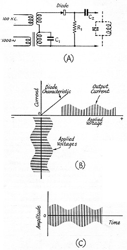
Fig. 3. A basic diode-modulator circuit is shown in (A). Ci and Ca are by-passes for the 100 kc signal.
The modulator action is shown at (B), where the envelope of the superimposed signals becomes a modulated envelope in the output. The a.c. coupling in the output of the modulator, and the tuned circuit, convert the "output current" envelope of (B) to the modulated-wave envelope of (C).
So far we have only half cycles of 100 kc r.f., all swinging up from zero to an amplitude determined by the 1000 cycle signal that was superimposed on the original signal. You know that half cycles of any frequency contain harmonics of that frequency, so we can expect that the current through R1 is made up of a 1000 cycle component, a 100 kc component, and some harmonies of 100 kc. (There are also those side frequencies we mentioned earlier, but they are close to 100 kc and its harmonics, and we will again ignore them in this discussion.) If now we connect a parallel circuit tuned to 100 kc on the other side of C2 (as shown by the dotted lines), only the 100 kc energy will appear across it, the other components being rejected by the selectivity of the circuit. The voltage across this tuned circuit will appear as in Fig. 3C, since the a.c. coupling (through C2) has made it necessary that each 100-kc. cycle swing as much below the axis as above. This figure we recognize as a modulated wave.
The diode characteristic shown in Fig. 3B is much too good to be true, and in practice it isn't a straight line from zero on up. A practical characteristic has some curvature, and so the usual practice in diode modulators is to use a large r.f. signal and a small audio signal. This has the effect of doing the actual work of modulating on a small relatively-straight portion of the diode characteristic, and simply means that you can't use a high percentage of modulation without running into distortion of the envelope. The same thing is true, of course, in plate-modulated Class C stages - you can't run high percentages of modulation without distortion - but there we don't worry about it so much. In the applications where diode modulators are used, we try to hold the distortion down as low as possible.
Balanced modulators
A balanced modulator is a device for obtaining the side-frequency components of modulation without passing the carrier. In single-sideband transmitters, this is done prior to removing one of the sidebands with highly-selective circuits. While balanced modulator., may take several different forms, they all serve the same basic purpose, and the various circuits involving diodes differ only in the frequency components (harmonics) that appear in the output.
The most common circuits are those shown in Fig. 4.(1) It is apparent in both that the carrier frequency cannot appear in the output because the net effect of the carrier across the output is zero, when there is no audio signal.
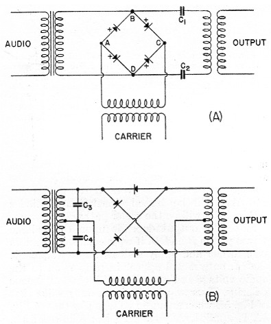
Fig. 4. The two common diode balanced-modulator circuits are (A) the bridge and (B) the ring. Condensers C1, C2, C3 and C4 are r.f. by-pass condensers, used to complete r.f. paths without short-circuiting the audio.
Now suppose that we disconnect the audio transformer and connect a small battery across points B and D in Fig. 4A, the positive terminal to B. Diodes AB and CD will be "biased back" by the amount of the battery voltage, and they will not conduct r.f. (of the proper polarity) until the r.f. voltage exceeds this bias value. The other two diodes, BC and AD, will conduct readily, however, and over more than half the r.f. cycle, because they are biased "forward." Since the one set of diodes is conducting better than the other, the circuit is no longer balanced, and r.f. will appear across the output. The fact that these are approximately half cycles of r.f. flowing through the diodes shouldn't bother you - remember that this is an a.c.-coupled affair and the r.f. will be normal full cycles in the output. The more voltage applied, the more the unbalance, and the more r.f. there is in the output. When the polarity of the bias is reversed, the diodes BC and AD will be biased "back," and diodes AB and CD will be the easier paths.
Since the output depends upon the voltage across points B and D, if we reconnect our audio transformer and apply a single audio frequency, the r.f. output will appear in proportion to the audio voltage and regardless of its instantaneous polarity. Thus we will obtain an output like that of Fig. 5B when an audio voltage like that of Fig. 5A is applied. Anyone who has followed s.s.b. testing techniques will recognize this pattern as that of the "two-tone" test signal, but it should be apparent to all how it is the envelope pattern of a balanced modulator when a single modulating frequency is used. It will also occur to the reader that the balanced-modulator action could have been described simply on the basis of a balanced bridge being upset by the action of the audio, without any introduction explaining something about normal modulators and a.c. However, the difference in envelope patterns between carrier and no-carrier signals is brought home a little better by running through the complete story.
Except that this isn't the complete story. One thing these envelope patterns can't show is the resultant frequency "spectrum" of the modulated wave, although the Handbook attempts to correlate the two.(2) For example, the frequency spectrum of the envelope shown in Fig. 5B, when generated in a balanced modulator, consists of two side frequencies, separated from the (eliminated) carrier by the modulation frequency. In the case we have been speaking about, the spectrum of this signal would show two side frequencies, 99 and 101 kc., with no energy at the (eliminated) carrier frequency of 100 kc. Such an envelope pattern can be generated in a normal modulator, by modulating with a complex wave that could be obtained from a full-wave rectifier and adjusting the modulation percentage to exactly 100. In this case, however, the spectrum would consist of the carrier at 100 kc and side-frequency components spaced at 1000 cycle intervals out to 10 or 15 kc either side of 100 kc. Hence, although the envelopes could look the same, the spectrums could differ greatly - the difference is in the phase of the r.f. cycles and the lack or presence of a carrier. In the balanced modulator, the phase of the r.f. in the output is reversed as the modulating signal passes through zero value, because the one pair of diodes takes over the job from the other, and routes the ri. differently from its source to the output trans, former.
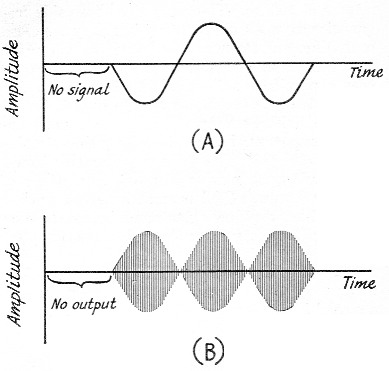
Fig. 5. A modulating signal as in (A) gives an r.f. output from a balanced modulator as in (B).
Practical considerations
It has already been mentioned that the ratio of modulating voltage to carrier voltage should be low in a diode modulator, if the distortion products are to be held to a low value, and this is equally true in the balanced-modulator application. Normal practice is to make the carrier voltage at least 10 to 20 times the peak modulating voltage. For germanium crystals and copper-oxide rectifiers, the r.f. voltage is usually on the order of 2 to 6 volts. The inherent carrier balance will sometimes run as high as 30 dB without any balancing adjustments, and with balancing (through circuits shown in any practical description) it will run to 60 or 70 dB Sideband energy is equal to the modulator power delivered, minus the resistance losses in the diodes, and these losses will run from 2 to 10 dB depending upon the carrier frequency. The rectifiers are in common use up to 4 Mc, and will be usable at higher frequencies with careful construction. A bugaboo at the higher frequencies is the variation in internal capacity of the rectifiers, and consequently they must be operated at lower impedance levels as the operating frequency is increased. From 600 to 1000 ohms is a practical level at 500 kc., but 50 to 100 ohms is recommended at 4 Mc.