S.S.B. exciter circuits using a new beam-deflection tube
Practical circuit data for modulation, frequency conversion and detection.
The new beam deflection tube described here appears to be a bulbful of versatility, with more applications than were visualized when the tube was under development as an improved type of balanced modulator. This article tells how the 7360 can be put to work in a number of ways in the amateur field, particularly in s.s.b. transmission and reception.
New beam-deflection tube, the RCA-7360, incorporates novel design features which, with suitable circuits, allow it to be used in many kinds of applications with improved performance at frequencies at least as high as 100 megacycles.
The tube was originally developed to provide a high degree of stable carrier suppression when used as a balanced modulator in single-sideband service. More than 60 dB of carrier suppression has been obtained with it as a balanced modulator in s.s.b. exciters of both the filter and phasing types. It is of course equally valuable in double sideband suppressed carrier service.
Frquency conversion, product detection, synchronous detection, single-ended to push-pull fase inversion, switching circuits, fader circuits and compressor-expander-limiter circuits are among the many other interesting applications in which the unique properties of this new tube have been found to be valuable.
In this article circuits will be described which make use of the 7360 as a balanced modulator, a frequency mixer and a product detector. Balanced modulator circuits will be shown for both the filter and phasing methods of s.a.b. generation. The circuits are presented for the purpose of illustrating various methods of employing this new tube as a balanced modulator and as a frequency mixer rather than as a complete s.s.b. transmitter design. The writer wishes to express his appreciation to M. B. Knight and Ken Uhler of RCA for much of the information in this article.
First, let's examine Fig. 1, which is a cross-section sketch of the main elements of the tube. The single flat cathode, control grid and screen grid form an electron gun which generates, controls and accelerates a ribbon or sheet beam of electrons. The screen grid and the two deflecting electrodes act as a converging electron lens to focus this beam.
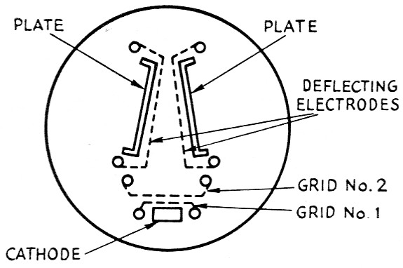
Fig. 1. Arrangement of electrodes in the beam-deflection modulator tube, type 7360.
Varying the bias or signal voltage on the control grid varies the plate current as in a conventional tube. The total plate current to the two plates, at a given plate voltage, is determined by the voltages applied to the control grid and the screen grid. The division of the total plate current between the two plates is determined by the difference in voltage between the two deflecting electrodes.
Mechanical-filter type S.S.B. generator
Now, bearing these brief fundamentals in mind, let's see how they can be applied in a balanced modulator, using a mechanical filter to obtain a single-sideband signal. A 455 kc circuit for this purpose is shown in Fig. 2.
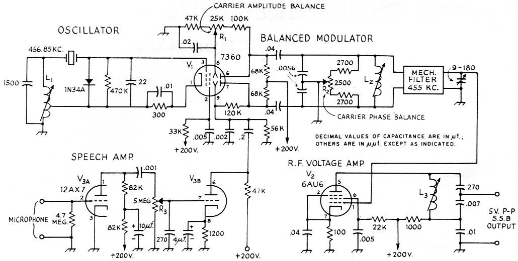
Fig. 2. Filter-type s.s.b. generator using the 7360 as a combined self-excited oscillator and balanced modulator. Fixed resistors are' Y2 watt except as indicated.
| L1 | App. 88 µH, adjustable (see text). |
| L2 | App. 50 µH, adjustable (see text). |
| L3 | App. 450 µH, adjustable. |
| R1,R2 | Composition control, linear taper. |
| R3 | Composition control, logaritmic taper. |
The 7360 beam-deflection tube as used in this circuit combines two basic functions - it generates its own 456.85 kc carrier as a crystal-controlled oscillator, and it also functions as a balanced modulator which delivers both sidebands without the carrier to the mechanical filter. The filter suppresses one sideband and delivers the other to its output circuit.
The control and screen grids of the 7360, together with its cathode, are used in a self-oscillating circuit. It is also entirely practical, of course, to supply the carrier to the control grid from a separate oscillator, if desired, as will be described later.
In the self-oscillatory circuit shown in Fig. 2 the 1N34A diode connected between the control grid and the ground side of the cathode-bias resistor acts as a clamp to prevent the voltage on the control grid from going positive or even to zero volts. As operated here the most positive excursion of the control grid is to -2.5 volt. This prevents excessive values of screen current from flowing and gives better modulation linearity and carrier frequency stability.
We now have a single-ended carrier input to our push-pull plate output. In order to suppress this carrier in the push-pull output circuit both ends of the output circuit must go equally positive and then equally negative at exactly the same times. That is, the amplitudes of the two voltages, one from each plate, must be exactly equal and the two voltages must be in exactly the same phase in order to balance out or cancel the carrier completely. Amplitude balance is obtained very simply by varying the d.c. voltage difference between the two deflecting electrodes by means of the amplitude-balance potentiometer, R1.
Since a phase unbalance of only 1 degree makes it impossible to obtain more than about 40 dB of carrier suppression, special pains were taken to provide good methods of obtaining stable phase balance. In the method used in Fig. 2 the phase angle of the load circuit is controlled by varying the resistance to ground from the two ends of the capacitance-center-tapped plate tank circuit by means of the phase-balance potentiometer, R2. This method is best suited for relatively low-frequency operation. A small differential capacitor across the plate tank circuit is best suited for phase balancing in higher-frequency circuits.
These two balance controls allowed better than 60 dB of carrier suppression to be obtained from the balanced modulator. An additional 20 dB of suppression was obtained in this filter circuit because the carrier was located at a point 20 dB down on the filter frequency-response curve. This gave a total of approximately 80 dB suppression!
Negative feedback
You will notice that each deflecting electrode receives its d.c. voltage (approximately 25 volts) from a tap on a resistance voltage divider from each plate to ground. A desirable by-product of this resistance coupling from plate to deflecting electrode is negative feedback. Additional negative feedback, which tends to correct any unbalance between the two plate currents, is obtained from the two 68,000-ohm plate resistors. If desired, still more negative feedback can be obtained by reducing the capacitance of the two 0.04-pf. plate blocking capacitors so that they offer a relatively high reactance to audio frequencies but relatively low reactance to the carrier frequency being used. This negative feedback improves modulation linearity and reduces hum and micro-phonics originating in the balanced modulator.
The audio signal is fed to this balanced modulator at a relatively high impedance - special transformers to obtain a low-impedance driving source are not required. Furthermore, a push-pull audio source is not required - a single-ended feed is used. With 10 volts r.f. on the control grid, 2.8 volts a.f. deflecting voltage is required. Both values are peak-to-peak.
This arrangement is possible because of the fundamental characteristic of the tube mentioned initially - the voltage difference between the two deflecting electrodes controls the division of the total plate current between the two plates. This gives an intrinsically balanced push-pull output from a single-ended input. Also, a 180-degree phase reversal can be obtained by simply switching the audio input from one deflecting electrode to the other.
In order not to overload the mechanical filter the gain of this circuit was reduced by shunting the mechanical filter input winding with a separate slug-tuned inductance, L2, as shown in Fig. 2. This allowed about 1.5 volts input to the filter. Approximately 0.5 volt peak-to-peak output was obtained from the filter.
This shunting inductance, L2, consisted of 63 turns of No. 36 enameled wire, close-wound in a single layer on a tube N2 inch in outside diameter. A 4-inch-diameter iron slug in the tube allowed the plate tank circuit to be resonated at the crystal frequency.
The tank. coil, L1, for the 456.85 kc crystal oscillator must be of the high-Q ferrite-core variety. One of the kind normally used as-an oscillator coil with the 6BE6 converter tube for the standard a.m. broadcast band was used in our tests. The cathode excitation can be obtained by a r tap on the coil. The cathode tap point should be rlocated above ground 13 to 15 percent of the total number of turns in the coil as a starting point. If possible, the r.f. voltage between grid and cathode should be measured with a high input-impedance v.t.v.m. equipped with an r.f. probe, and the tap point varied so as to obtain 10 volts r.f. peak-to-peak (3.5 volts r.m.s.) between the grid and cathode.
When using 1500 pF total oscillator tank capacitance, provision should be made for varying the coil inductance above and below about 88.5 µH by a percentage a little larger than the capacitance tolerance percentage of the tank capacitor used, in order to resonate the coil-capacitor combination at the crystal frequency. Varying the tuning of the tank circuit around the resonance point will vary the oscillator frequency slightly.
Voltage amplifier
A voltage amplifier suitable for raising the 0.5-volt output from the mechanical filter to a more usable level consists of a 6AU6 stage, Fig. 2, that has a capacitance voltage divider as a part of its plate tank circuit. With the constants shown, it can provide an s.s.b. peak-to-peak output of about 5 volts. However, any output up to about 150 volts can be obtained by changing the capacitance ratio of the two voltage-divider capacitors that are connected in series across the 6AU6 plate tank circuit. When this ratio is changed the resultant capacitance of the two capacitors in series must remain constant so the L/C ratio of the tank circuit is not changed too much.
V.F.O.-Mixer circuit
Fig. 3 shows a schematic of a v.f.o.-mixer unit. Its resemblance to the balanced modulator circuit is quite evident. Here the front end again functions as an oscillator, except that it is of the variable-frequency type.
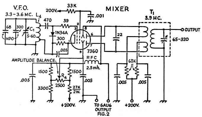
Fig. 3. Combined v.f.o. mixer for frequency conversion from 455 kc to 3.8 - 4.0 Mc. Fixed resistors are ½ watt except as indicated. Decimal values of capacitance are in µF others are in pF.
| C1 | Variable, 5-60 pF. |
| L1 | See text. |
| R4 | Composition control, linear taper. |
| T1 | See text. |
The modulating signal is the s.s.b. output from the 6AU6 stage described above. Again the modulation is applied to only one deflecting electrode, the other being at r.f. ground due to the 5 nF bypass capacitor.
The mixer tank circuit employs a center-tapped, bifilar-wound inductor with the 68,000 ohm feedback resistors in its center-tapped connections to the d.c. plate voltage supply. This mixer output transformer, T1 in Fig. 3, was constructed as follows for our tests on 3.9 Mc.:
Primary - Bifilar-wound on ½ inch diameter tube, tuned with a ¼ inch slug; winding length, 3/8 inch. Two wires wound parallel to each other on tube, 23½ turns of each wire (47 total). No. 34 wire, single Teflon insulation if possible (silk insulation can be used if necessary). The dielectric properties of the insulation on the wire are important because in a bifilar winding the distributed capacitance is relatively high and is a part of the tank capacitance. This accounts for the relatively low value of 22 pF shown for the tank capacitor in this circuit.
Secondary - Twenty-six turns of No. 32 wire with Formex insulation, close-wound in a single layer. The spacing of this winding from one end of the primary winding should be adjusted so as to obtain satisfactory bandpass between 3.8 and 4.0 Mc. Approximately 190 pF was required to resonate the secondary to 3.9 Mc.
Without the carrier amplitude-balance control, R4, shown in Fig. 3, the balanced load circuit provides 20 to 25 dB suppression of the v.f.o. carrier. Including the carrier amplitude-balance control allows about 40 dB total v.f.o. carrier suppression, thus simplifying the selectivity requirements of the output circuit.
The grid and cathode connections of the v.f.o. are tapped down on the inductor so as to reduce the coupling between the tube and the tank circuit, and thus improve stability and obtain the correct r.f. voltages on the tube elements.
The v.f.o. tank coil, L4 in Fig. 3, consists of 15 turns of No. 22 enameled wire spaced uniformly in a winding 0.6 inch long on a 1-inch diameter coil form. No slug was used. The grid tap should be located 7½ turns above the ground end of the coil. The cathode tap is 1_9/16 turns above the ground end of the coil. Actually, in building L4, it was first determined that the coil specified above required a total length of wire measuring 121 cm. The taps were then soldered to this length of wire before winding it on the coil form, in order to avoid melting the polystyrene form with the hot soldering iron. The cathode tap was located 15.1 cm (12½ per cent of the total wire length) from the ground end of the wire and the grid tap was located 60.5 cm (50 per cent of the total wire length) from the ground end. At 3.5 Mc this coil had a Q of 150 and required 400 pF to resonate it. The Q was measured with the coil shield in place.
7360 Mixer With Separate Oscillator
A generalized mixer circuit for use with an external r.f. oscillator is shown in Fig. 4. Here the s.s.b. input is shown fed from a two-winding transformer instead of from a capacitive tap on the preceding tank circuit, as was used in Fig. 2.
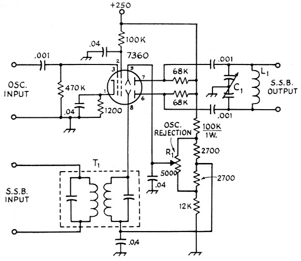
Fig. 4. Balanced mixer circuit with separate excitation. Capacitances are in µF; fixed resistors are ½ watt except as indicated. Tuned-circuit constants depend on frequency; ordinary L/C ratios may be used for L1C1 and in the s.s.b. input transformer, T1. R1 is a linear-taper composition potentiometer.
Since the 7360 is not used as a self-oscillator the 1N34A diode clamp is not used and the cathode bias resistor is changed from 300 ohms to 1200 ohms. The r.f. oscillator input to the control grid must be adjusted to be between 5 and 10 volts peak-to-peak, measured between control grid and cathode, for best results. A 40 nF r.f. bypass capacitor effectively grounds one deflecting electrode (pin 9) so the s.s.b. input is single-ended between the other deflecting electrode and ground.
In this mixer circuit the 68,000-ohm d.c. feedback or plate-current equalizing resistors are connected as shunt feed resistors to the two plates, the same as was shown in the balanced modulator circuit in Fig. 2, instead of being in series with the center-tapped connections to the d.c. plate voltage supply as was shown in the mixer circuit of Fig. 3. This difference allows L1, the mixer plate tank coil, to be a simple untapped coil instead of requiring a bifilar-wound coil as is the case when the d.c. feedback resistors are connected in series with the split, center-tapped coil connections to the plate voltage supply. The capacitance and inductance values of T1 and C1 and L1. in Fig. 4 will depend upon the input and output frequencies involved.
The combination of the two circuits shown in Figs. 2 and 3 will provide single-sideband output in the range between 3.8 and 4 Mc. Since these circuits were for the purpose of obtaining characteristics and specifications, as was previously stated, they do not include all of the facilities that might be required for actual amateur operation on the air, particularly as regards switching between upper and lower sideband.
Sideband switching can be obtained by any of the normal methods. For example, a simple method would be to employ two crystals in the carrier oscillator circuit of the balanced modulator, one for upper sideband and the other for lower sideband, with a switch for instant choice. Band switching would require an additional mixer stage to heterodyne the v.f.o: mixer output to the various other bands.
R.F. phasing-type S.S.B. generator
Fig. 5 shows the schematic of an r.f. phasing exciter circuit for 455 kc. which gives a peak-topeak output of about 4 volts single sideband. Here you see the usual r.f. and a.f. 90-degree phase-shift networks, an audio amplifier, and two 7360 tubes as balanced modulators.
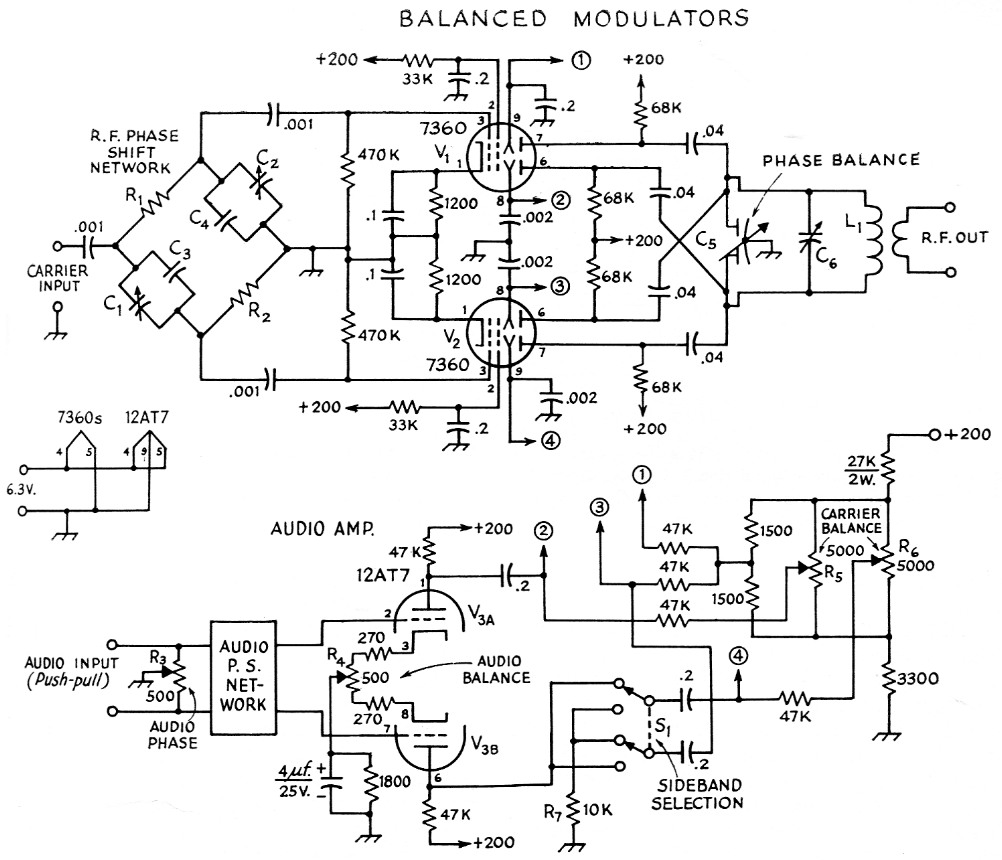
Fig. 5. Phasing-type s.s.b. generator using two 7360s as balanced modulators. Capacitances are in pF; fixed resistors are ½ watt except as indicated.
| C1,C2 | Trimmers, ceramic or air, approximately 25 pF. |
| C3,C4 | Value dependent on frequency and R1 R2. Reactance at operating frequency should be approximately equal to the resistance of R1 and R2. |
| C5 | Differential capacitor, approximately 25 pF per section. |
| C6 | Variable, to resonate with L1 at output frequency. |
| L1 | To resonate with C6 at output frequency. Conventional L/C ratio may be used. |
| S1 | D.p.d.t. toggle or rotary. |
| R1,R2 | Non-inductive, ½ or 1 watt, values to be equal within close tolerances. Actual resistance not critical, but should be low to minimize effect of stray capacitances. Resistances of the order of 100 ohms are satisfactory. |
| R3,R4 | 500 ohm composition control, linear taper. |
| R5,R6 | 5000 ohm composition control, linear taper. |
| R7 App. | 10,000 ohm, ½ watt (see text). |
The audio circuits include two sideband-balance potentiometers - one for adjusting the input voltage ratio to the audio phase shift network, R3, and one for audio amplifier balance, R4. Each balanced modulator has its own carrier amplitude-balance potentiometer which controls the d.c. bias voltage on one of its deflecting electrodes, as was done in the filter rig.
The outputs of the two balanced modulators are combined in a common push-pull tank circuit. Over-all r.f. phase balance is obtained in this tank circuit by the use of a differential capacitor connected across the tank circuit. This type of phase-balancing circuit is better suited to the higher carrier frequencies generally used in phasing-type exciters.
The r.f. phase-shift network used here is of the simple R-C bridge variety. Any of the other usual types of networks could be employed instead if desired.
As in the filter exciter, better than 60 dB suppression of the carrier was obtained by proper adjustment of the r.f. phase and amplitude balancing controls.
Suppression of the unwanted sideband is limited by the degree of accuracy with which the audio phase-shift network maintains an exact difference of 90 degrees in phase between the two branches of the audio system, over the entire range of audio frequencies fed to the audio phase-shift network. With the audio phase-shift network used in our experimental setup carrier plus unwanted sideband measured about 40 db. below the wanted sideband.
Switching the single-ended audio input to one of the balanced modulators from one deflecting electrode to the other allows a ready choice of upper or lower sideband output. This is done by switching the audio input to one balanced modulator, V2, from one deflecting electrode to the other, through one arm of S1. The other arm of Si connects a 10,000-ohm resistor, R7, between the other deflecting electrode and ground through a d.c. blocking capacitor, in order to preserve better balance. The exact value of R7 should be adjusted for best balance stability since various wiring layouts, and particularly various audio tube types, will require different values.
As in the case of the filter circuit, additional stages and functions would be required for a complete s.s.b. exciter, including a v.f.o.-mixer stage and a crystal oscillator-mixer stage to heterodyne the signal to various bands.
7360 as a product detector
A rather unique circuit for obtaining a single-ended audio output from the 7360 as a product detector in a receiver is illustrated in Fig. 6. As in the v.f.o. circuit of Fig. 3, the "front end" of the 7360 is used as a self-oscillating b.f.o. and includes the diode clamp to prevent its control grid from going positive. A fairly high-Q, high-C b.f.o. tank circuit is used, and with the coil tapped as in Fig. 6 about 8 volts peak-to-peak was obtained between control grid and cathode.
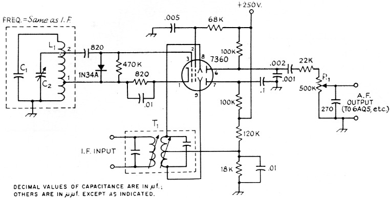
Fig. 6. Product detector circuit with self-excitation. The beat-frequency oscillator tuned circuit, C1C2L1, should be high-C at the intermediate frequency used; C2 is for fine frequency adjustment. On L1, tap 1 is at approximately 5 per cent of the turns counted from ground, and tap 2 at approximately 25 per cent. T1 is an i.f. transformer with balanced secondary, such as is used for a push-pull diode detector. Ri is the audio volume control.
The deflecting electrodes were driven in push-pull primarily because it was felt that limiting of high-amplitude impulse noise would be better. Actually, tests with the same circuit connected for single-ended input to one deflecting electrode showed no substantial difference. Balanced operation has some second-order advantages, however, such as minimizing the contribution of stray capacitance to oscillator locking or pulling.
The i.f. input to the deflecting electrodes should be held close to 10 volts peak-to-peak. At higher inputs the output "flattens" noticeably. If the input signal is held close to this maximum the flattening characteristic will limit impulse-noise peaks.
As indicated in Fig. 6, the b.f.o. and audio output of one plate is bypassed to ground through a 0.1-µf. capacitor. A 0.001-µf. capacitor to ground from the other plate bypasses the b.f.o. output to ground while the audio output (more than 20 volts at maximum input signal) is used to drive the grid of a 6AQ5 output tube. This circuit was tested at an intermediate frequency of 910 kc. (the output from a BC-348M receiver). It is probable that more of an r.f. filter may be required at lower intermediate frequencies. For example, the 22,000-ohm r.f. filter resistor may need to be replaced with an i.f. choke.
Maximum suppression of the i.f. in the audio output of the 7360 plate circuit could be obtained by using a push-pull or balanced output circuit together with an amplitude-balance potentiometer on one of the deflecting electrodes, as is shown in Fig. 4.
H.C. Vance, K2FF.