How to stabilize your transistorized equipment
Fixing the operating point in the presence of temperature and transistor variations.
Transistors are far more sensitive to temperature than are vacuum tubes, and no transistor circuit design is considered satisfactory that does not include provision for overcoming the effects of temperature variations over a reasonable range. This article discusses stabilization principles and describes practical circuit design methods.
Many amateur-designed transistor circuits do not take into consideration the effects of transistor production variations or the effects of temperature on transistor parameters. While some amateur equipment is not called upon to perform under severe environmental conditions, certain transistor parameters suffer comparatively large variations with small changes in temperature. Mobile amateur equipment is subject to variations in temperature from below freezing to as high as 150 degrees F. Portable equipment, too, is required to operate over a wide range of temperatures. Even in the shack, if a transistorized unit is placed on top of a piece of equipment which generates heat it may fail if not temperature-stabilized or compensated. Perhaps the most important consideration of all is the fact that in case of emergency or disaster, conditions are usually much less ideal than in our normal operating sessions.
Production variations between transistors of a given type are very large compared with those of vacuum tubes. These variations are wider in the lower-priced experimenter and entertainment grades than in the more expensive commercial and military types. The practice of designing for temperature stability has the additional advantage that it makes the circuit more tolerant of production variations between transistors. This minimizes the necessity for hand-tailoring circuits - that is, designing them around the particular transistor to be used.
Another bonus is that burnouts and thermal runaway are virtually eliminated.
The old saw, " You can't get something for nothing," applies to some degree. The price we must pay is greater circuit complexity, higher current drain, and sometimes a loss in performance.
Silicon transistors are usable at higher temperatures than germanium units, but carry a much larger price tag. The principles described in this discussion apply equally as well to silicon types as to the germanium units.
Leakage Current
Before we can compensate for variations, we must know what is varying. The worst offender with which we must contend is the leakage current, designated Ico. In normal operation the base-collector junction is reverse biased - that is, the polarity of the battery source is applied in the nonconducting direction. All semiconductor junctions have a leakage current which flows in the reverse direction to normal conduction. In the case of the transistor this current flows between the collector and base. If the supply voltage is applied between collector and emitter - as it is in a grounded-emitter stage - with the base open-circuited, this leakage current must also flow through the base region to the emitter. See Fig. 1. Current flow from base to emitter acts as a forward bias on the transistor, and by transistor action this causes a collector-to-emitter current to flow. The magnitude of this collectorto-emitter current is equal to the base current multiplied by the current gain, β, of the transistor. Therefore, the total collector current, Ic, is the sum of the collector-to-base current, Ico and the collector-to-emitter current, ΓIco: Ic = Ico + βIco.
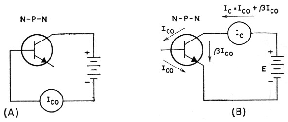
Fig. 1. Transistor leakage current, Ico.
(A) How it is measured;
(B) How it affects the collector current, lc.
In germanium transistors Ico, increases approximately 10 per cent per degree Centigrade. This amounts to doubling Ico for an 18 degree Fahrenheit rise. If β would remain constant over this range, Ic would also double for an 18 degree rise; that is, substituting 2Ico for Ico in the equation above:
Ic = 2Ico + β(2Ico) = 2(Ico + βIco)Unfortunately, β also increases with temperature, although at a lower rate than Ico. To illustrate the rapid change of collector current with temperature in Fig. 1, let's take an example:
A transistor at 72° F has β = 50, Ico = 10 µA . It is connected as in Fig. 1B with a 10 volt supply. What collector current will flow?
Ic = Ico + βIco = 0.01 + 50(0.01) = 0.51 mA.
What current will flow at 90° F, assuming that β increases 1 per cent per degree F?
At 90° F. β = 50 + (0.01) (90 - 72) (50) = 50 + 0.18(50) = 50 + 9 = 59
Ico = 2 × 0.01 = 0.02 mA.
then
Ic = 0.02 + 59 (0.02) = 1.2 mA at 90° F.
The internal impedances of a transistor also vary with temperature, but the variation is less than with β or I0°, and does not have as profound an effect on circuit performance. Note that increasing temperature tends to increase the collector current, therefore we must take steps to prevent this current from getting too far from the original operating point within the temperature range we expect to meet. This will be the aim in the principles to follow.Design principles
Here are five general rules to apply to transistor circuits to minimize the effects of temperature changes:
- Limit the temperature range.
- Provide a degenerative d.c. path around the stage.
- Keep d.c. resistance in the base circuit as low as is practical.
- Use temperature compensation.
- Use balanced circuitry to cancel variations caused by temperature changes.
Rules, 1, 4 and 5 could each provide enough material for discussion to fill an article the size of this one. Here the emphasis will be placed on Rule 2, with a preliminary brief discussion of the others.
1. Limiting the temperature range
This is perhaps the thing over which we have the least control. However, we can avoid mounting transistors near tubes, resistors, and other components that get hot. In the case of a mobile rig, keep the transistorized units away from the engine, direct sunlight, and other heat sources. Sometimes the critical problem arises from heat generated within the transistor junction itself. In this case it is necessary to provide a heat sink to conduct heat away from the junction as rapidly as possible. Ventilation, heat-radiating fins and dull black paint, even the use of blowers, should not be overlooked.
3. Keep D.C. Resistance in Base Circuit Low
The example in connection with Fig. 1 illustrated the evils of an open base circuit. If the base were grounded, I. would become I,. and it would be independent of β. Of course, such a circuit wouldn't amplify, either, but the lower the resistance we can insert between base and ground the more we reduce the temperature dependence. In the case of R-C coupled audio stages this will reduce the gain since the resistance will load the input-signal source. A transformer-coupled stage (a.f., i.f., or r.f.) could provide for a d.c. short circuit to ground with no loss in gain (this is mentioned by way of example only, since the stage still must have forward bias applied if it is to operate Class A).
4. Temperature compensation
This refers to the practice of using a temperature-sensing device to vary a voltage, current or resistance in such a way as to cancel the effects of temperature changes, as opposed to stabilizing against them. Temperature compensation is applied principally in circuits which are required to handle large amounts of power, and where efficiency is a prime consideration. It also finds application in correction for drift in d.c. amplifiers.5. Balanced circuitry
Here is another broad area which finds limited application in amateur equipment. It is useful in d.c. amplifiers, especially at low levels. This is where having transistors of both p-n-p and n-p-n types becomes advantageous.
2. Degenerative d.c. path
This heading could be deceptive. The principle is not limited to one stage - in fact, it is more advantageous when applied over more than one stage - but circuit analysis of multiple stages with feedback becomes considerably more complicated than that of a single stage. Also, trialand-error procedures should be left to the experienced - unless you have a large supply of transistors with which to gain the experience. This discussion will be confined to a single stage.
Fig. 2 shows different configurations for a single Class A audio stage. They are in approximate order of increasing stability, the first (A) being an unstabilized stage, and the last (F) being the most stable. The equations accompanying each circuit can be solved for the necessary resistance values. The supply voltage must be known, the operating point (collector current) determined, and RG chosen.
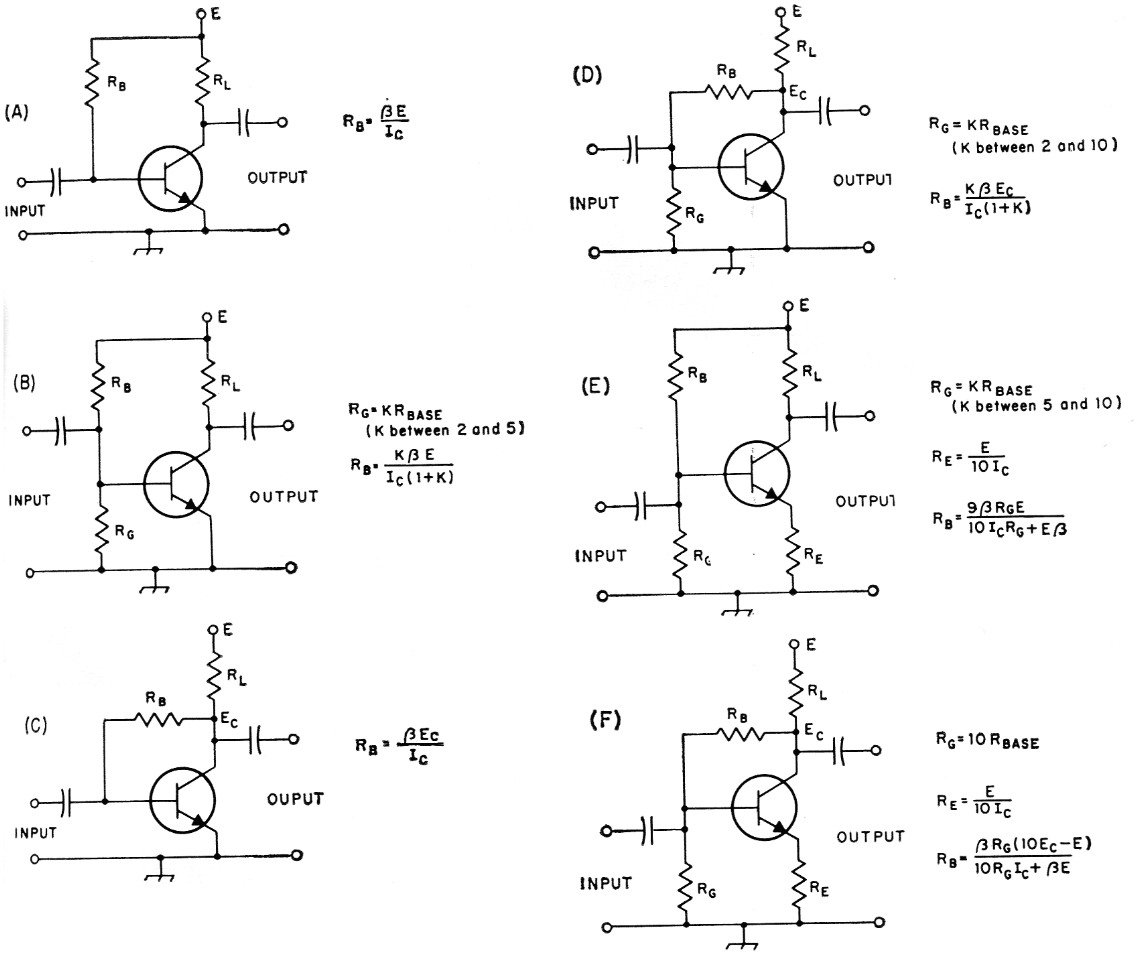
Fig. 2. Bias stabilization circuits for resistance-coupled amplifiers. Equations are based on the assumption that Ico is small at room temperature; in circuits D, E, and F this assumption is valid, but in circuits A, B, and C the value of RB will have to be adjusted if Ico is high.
An approximate value for the load resistance, RL, is E/2Ic (Ic = collector current) although other values may be used to meet specific circuit design requirements, in which case the proper value may be determined from the transistor characteristic curves. When RL = E/2Ic the collector-to-ground voltage, Ec, is approximately equal to one-half the supply voltage; with other values of RL, Ec can be found from the curve data.
The value of RG may be selected arbitrarily, but should be within the limits shown. RBASE is usually of the order of 1000 ohm.
RG fixes the base circuit resistance; therefore, in accordance with Principle (3), it should be as low in value as is practical. Its value will depend on the base input resistance of the transistor used, the degree of stabilization required, and which circuit is used. Some ballpark indication of the value to use accompanies each circuit. Use lower values for portable and mobile gear, and higher ones for home-station use. If there is doubt as to what operating point to use, consult the transistor ratings for typical operating conditions.
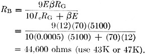
Here is an example to show how the equations are used:
A 2N591 transistor (β = 70, RBASE = 1000 ohm) is to be used as the first stage in a speech amplifier for a mobile rig. (When the transistor data sheets show maximum, design center, and minimum values for β, always use the minimum value unless you happen to know the actual value of β for your particular transistor.) The battery voltage is 12. Find values of the resistances to be used, the circuit chosen being that of Fig. 2E.
1) Choose operating point and RL. From transistor data, Ic = 0.5 mA. A suitable value for R1, is 10,000 ohm.
2) Choose RG equal to 5RBASE = 5(1000) = 5000. Use the nearest standard value, 5100 ohm.
3) Find RE:
![]()
4) Find RB:
For maximum gain, the emitter resistor, RE, would be bypassed for audio frequencies. The size of the bypass should be such that its reactance at the lowest audio frequency to be amplified is low compared with RE. In this case, for a low frequency of 300 c.p.s. a 10 µF. bypass would be satisfactory. The resulting schematic of the stage is shown in Fig. 3.
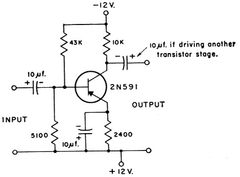
Fig. 3. Example of circuit values based on the circuit of Fig. 2E. With this stabilization the amplifier will operate over a temperature range from below freezing to above 150° F.
The circuits shown in Fig. 2 can be adapted to transformer coupling as shown in Fig. 4. The transformers could be for either audio, i.f. or r.f. amplification. Note the use of bypass capacitors and transformers to keep the a.c. and d.c. paths independent of each other. Conventional practice in receiver a.v.c.-controlled i.f. stages calls for lifting RG from ground and returning it to an a.v.c. line. The d.c. equivalent circuit for an oscillator would be the same as for the circuits of amplifiers. The a.c. configuration would have one transformer with a feedback winding. Figs. 5A and 5B show two arrangements.
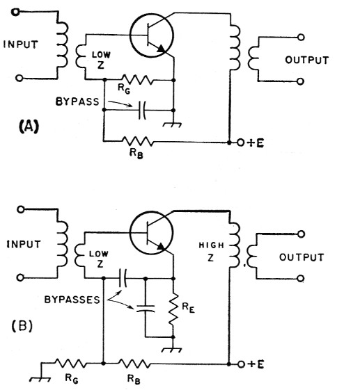
Fig. 4. Transformer-coupled circuits suitable for audio, i.f. and r.f. amplification. The bias stabilization in (A) corresponds to that of Fig. 2B; (B) corresponds to Fig. 2E.
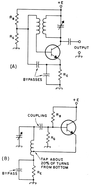
Fig. 5. Oscillator circuits. A) Tickler circuit; (B) Hartley Stabilization in both circuits is the same as Fig. 2E. Use equations given in Fig. 2E except that RG should be equal to RBASE in (A) above, and RG should be 5 to 10 times RBASE in (B) above.
The circuits in Figs. 2E and 4B are recommended for general use. The unstabilized stage of Fig. 2A should not be used in the final design of any equipment. It might be appropriate at this time to point out that transistor characteristics also vary with age, especially during the initial period of service. If the circuit of Fig. 2A is used RB might require readjustment after a few weeks of operation.
The circuits outlined in this discussion do not apply to power converters or power amplifiers where efficiency is important since the losses in the series resistances would be intolerable. Neither do they apply to d.c. amplifiers, since the d.c. degeneration would reduce the gain as much as it would improve the stability. These and certain other transistor applications must be handled by the other methods mentioned earlier.
It is hoped that the principles, circuits and design equations described will be of help to amateurs wishing to "take a whack" at designing their own transistor circuits.
Gilbert L. Boelke, W2EUP.