The design of regulated low-voltage power supplies
Stable A.C. operated power source for transistor circuits.
Batteries, fixed low-voltage supplies, and bleeder networks on high- voltage supplies designed for use with vacuum tubes all have obvious shortcomings when used by the experimenter to power transistor circuits. A variable, regulated, low-voltage power supply eliminates the problems associated with the above sources. This article deals with the in general design of such devices and a specific example which can be duplicated at a very modest cost with reliable results.
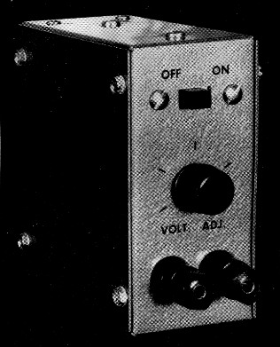
This regulated supply for use with transistors is enclosed in a 4 × 4 × 2 inch aluminum utility box.
There is no difference between the principles involved in voltage-regulated power supplies using vacuum tubes and those upon which similar circuitry using transistors operate. The only differences lie in the components used and the voltage levels involved. The block diagram of Fig. 1 shows the essential elements in a series regulator of conventional type. To analyze the operation of this circuit, consider first that the supply is operating at a preset output voltage and, for one reason or another, this voltage decreases. The voltage comparator senses the change in output voltage by comparison with a stable voltage-reference element, producing an output signal related to this change which drives the d.c. control amplifier. The control amplifier in turn amplifies this signal and, by its output, controls the resistance of the series element (in this case reducing it) to restore the output voltage to its original value. If for some reason the output voltage should increase, the same sequence of events would occur, except in the opposite phase. This will result in an increase in the resistance of the series element with a corresponding decrease in the output voltage to its original value.
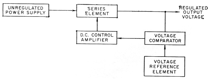
Fig. 1. Block diagram showing the essential elements of a voltage-regulated supply.
Since a change in output voltage is required to produce a change in the resistance of the series element, this type circuit cannot completely compensate for output changes. However, the greater the gain of the loop consisting of the voltage comparator, d.c. control amplifier, and series element, the greater will be the compensation. The upper limit of the gain usable in this loop is determined by stability considerations. If an attempt is made to use too much gain without compensating for phase shift at the higher frequencies, the circuit will become regenerative and oscillations will result, making the supply useless for most applications. The frequency response of this feedback loop normally extends well beyond the attendant ripple frequency of the unregulated power supply, hence the output voltage from this type of regulator is extremely smooth and ripple free.
Zener diode as reference
A more detailed description of a transistorized regulator can be made using the circuit diagram of Fig. 2. Although most low-priced regulators will use p-n-p transistors, Fig. 2 has been drawn with n-p-n units to facilitate the discussion and to make it easier for one who is more familiar with vacuum-tube circuits to make the transition. A 1-to-1 correspondence exists between the circuit elements of Fig. 2 and the blocks of Fig. 1. The reference element is the zener or breakdown diode, CR1. When subjected to a reverse voltage greater than its breakdown potential, Vz, a diode of this kind maintains a constant terminal voltage which is relatively independent of the current which passes through it. Thus its action is much like that of the familiar VR tube with the important exception that its breakdown and operating voltages are one and the same as opposed to the VR tube which requires an ionizing voltage considerably greater than its operating voltage. As in the case of the VR tube, its operat ing current range is rather restricted. The limiting factor in determining the maximum current through a zener diode is its maximum allowable dissipation, typically 200 to 500 mW for the pigtail variety. For maximum. stability it is important not to operate these diodes near their power limit since they are tehperature sensitive and the heat produced by their own power dissipation will affect the breakdown potential.
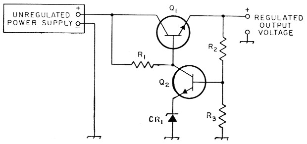
Fig. 2. Regulator circuit using transistors. Circuit designations are for text reference purposes.
Transistor regulator
The comparator circuit is the base-to-emitter junction of transistor Q2, the control amplifier. The controlled series element is Q1, normally a power transistor. R2 and R3 are used as a divider across the output voltage so that the regulator can be adjusted for an output greater than the zener voltage of CR1.
In the following theory of operation two particular approximations have been used. First, that the base-to-emitter drop Of Q2, normally on the order of 0.2 volt, is negligible and, secondly, that the base current of Q2 flowing through R2 does not produce a significant voltage drop. The latter will be true for all intents and purposes provided that the bleeder current through R2 and R3 is several orders of magnitude greater than the base current of Q2.
In operation, the voltage at-the base of Q2 is the zener voltage of CR1. Taking into account the divider action of R2 and R3, the output voltage will then be found from
![]()
Thus, by varying the ratio of R2 to R3, the output voltage can be adjusted between a lower limit of Vz and an upper limit determined by the unregulated input voltage and the voltage ratings of the circuit components.
If the output voltage of Fig. 2 were to increase because, for instance, of a decrease in load current, the base current of Q2 would necessarily increase, resulting in an amplified increase in the collector current of Q2. This increased current flow through R1 causes a drop in the base voltage of Qi and a corresponding increase in the effective resistance of the oollector-to-emitter circuit of the series element QI. The end result would be a reduction in the output voltage to its preset value. An analogous series of events will occur to raise the output voltage to its original value should something, say a decrease in line voltage, cause it to be lowered.
Transistor protection
The most serious shortcoming of a regulator of this sort using a power transistor as the series element is the possible destruction of Q1 by an accidental overload or short circuit of the output. If the output terminals are shorted in the circuit of Fig. 2, practically the only impedance to the flow of current through Q1 will be the internal impedance of the unregulated supply, usually a matter of ohms, probably resulting in the almost immediate destruction of Q1. It should also be noted that an output short would instantaneously apply the full output voltage of the unregulated supply from collector to emitter of Thus, if the voltage rating of Q1 is less than the output voltage of the unregulated supply, the chances of the survival of Q1 are just about nil. Because of the inherent time lag of fuse elements and circuit breakers they can offer protection only from overloads of the regulator which are still within the ratings of Q1.
Many sophisticated circuits have been devised to protect the series transistor, but most of these add seriously to the complexity and/or cost of the basic regulator. A simple yet extremely reliable means of protecting Q1 from being destroyed by current overloads or output shorts is to increase the output impedance of the unregulated supply by connecting a power resistor between the unregulated output and the collector of Q1. The decrease in circuit efficiency and regulation can be considered negligible when compared to the resulting circuit protection. This device has been used with gratifying results in regulators rated as high as several amperes. This technique will not protect Qi from voltage overloads. The simplest expedient here is to select a transistor with a voltage rating sufficient to withstand the full voltage of the unregulated supply.
There are two criteria used in selecting the value of the protective resistance. First, it should be large enough to limit the current through Q1 to a safe value in the case of a short across the output of the regulator. Secondly, it should be small enough so that under the conditions of maximum rated regulator output voltage and current, and minimum line voltage, the valleys of the voltage waveform at the collector of Q1 are at least 2 volts higher than the output of the regulator. The latter is necessary to maintain regulator action throughout the complete cycle of input voltage.
Practical Regulated Supply
The circuit of a versatile yet simple regulated power supply that can be duplicated for less than twenty dollars at mail-order prices is shown in Fig. 3. This circuit varies only in detail from the basic circuit of Fig. 2. The current-limiting resistor, R5, discussed above, has of course been added between Q1 and the unregulated supply. R6 has been added to supply current to CR1, the zener diode. If this supply were to be used at a fixed output voltage of about twice the zener voltage or higher, better regulation would result by connecting the left-hand end of R6 to the negative output terminal of the regulator rather than to the unregulated supply voltage. In this case, R6 should be of such a value as to provide about 5 or 6 mA to CR1. Q1 and Q3 are connected in what has come to be known as a Darlington pair. As a first approximation, Q3 can simply be considered as a current amplifier which also raises the base input impedance of Q1 as seen by the collector circuit of Q2. C2 and R4 have been added to eliminate a high-frequency oscillation which occurred due to phase shift within the feedback loop. C3 helps to improve the transient response and R2 has been made variable to provide a means for adjusting the output voltage. C4 reduces the ripple voltage across the reference diode and hence the ripple in the regulator output. The addition of R7 prevents Q3 from being cut off at low output currents.
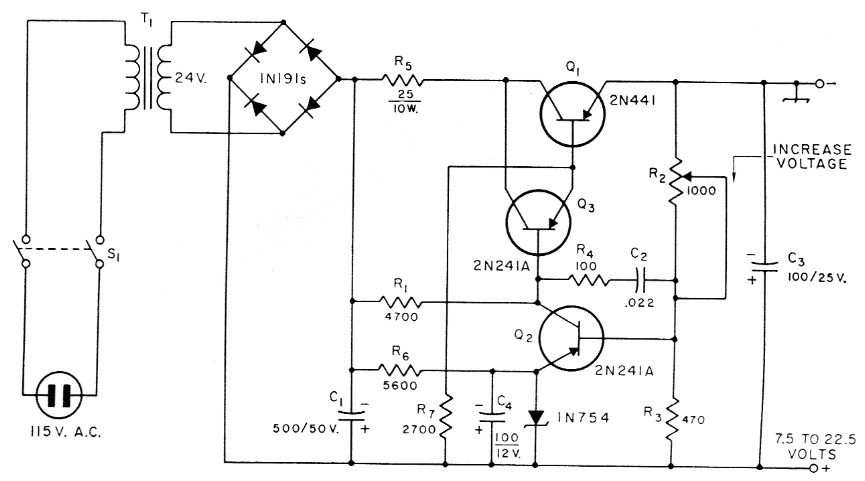
Fig. 3. Circuit of the transistor-regulated supply. Capacitances are in µF and capacitors marked with polarity are electrolytic. Resistances are in ohm and resistors are ½ watt unless indicated otherwise. Except as listed below, circuit designations are for text reference purposes.
| CR1 | 1N754 zener diode (Texas Instruments). 6.8 V, 400 mW |
| Q1 | 2N441 (Delca). Q2, Q3-2N241A (G.E.) |
| R2 | Wire-wound control, linear taper. |
| S1 | D.p.s.t. slide switch. |
| T1 | 24 volt 0.3 ampere filament transformer (BursteinApplebee cat. No. 601, part No. 18B506). |
Construction
The only precautions to be observed in constructing this and similar regulators are that the heat-producing elements, such as R1 and Q1, are not in a position to cause heating of the low-power transistors, Q2 and Q3, or the zener diode CR1, and that Q1 is mounted to an adequate heat sink. Several of these units have been built completely within 2 × 4 × 4 inch utility boxes with heat sinks of only 2½ × 1½ × ¼ inch aluminum with completely satisfactory results. The characteristics of one of these units are shown in Table 1.
Other output ratings
Changes in the output voltage and/or current ratings of the circuit of Fig. 3 can readily be made. As previously mentioned, the lower limit of the output voltage is determined by Vz, hence lower output voltages would require a zener diode with a breakdown voltage of several tenths of a volt less than the minimum output voltage required. If this minimum is less than 4 volt, a haft with its negative terminal connected to -the emitter of Q2 can be substituted for the zener diode. This is necessary because zener diodes with a breakdown voltage less than about 3.5 volt are not available. if this substitution is made, R6 and C4 may be deleted. The use of a battery in place of the zener diode is, of course, not restricted to extremely low-voltage supplies, but is an expedient that can be used at any voltage level to reduce cost by a couple of dollars or so. If drastic changes in the voltage range are contemplated, changes in Ri and R6 may be required. 116 should be selected to supply in the neighborhood of 5 mA to the zener diode. A value of R1 should be determined that will keep the collector current of Q2 in the 1 to 5 mA range.
If the current ratings of the regulator are to be increased much beyond those indicated in Table 1, Q1 should be fastened to an adequate heat sink and Q3 should be changed to a medium-power unit. The current rating can be further increased by paralleling Q1 with another similar unit. If this is done, it is a good practice to include equalizing resistors in each of the Q1 emitter circuits. The value of this resistor is selected to drop about 1 volt under full load.
| EO V | IO1 mA | EAC2 mV R.M.S. | E13 mV | E24 mV |
|---|---|---|---|---|
| 7.5 | 300 | 3.3 | 75 | 25 |
| 10.0 | 250 | 4.2 | 85 | 30 |
| 12.5 | 230 | 4.6 | 95 | 35 |
| 15.0 | 170 | 5.0 | 100 | 45 |
| 17.5 | 135 | 5.3 | 100 | 55 |
| 20.0 | 100 | 6.0 | 100 | 65 |
| 22.5 | 90 | 8.0 | 110 | 90 |
| 1 Maximum load current with 115 V a.c. input. | ||||
| 2 Output ripple voltage at maximum load, 115 V a.e. input. | ||||
| 3 Change in output voltage as output current is varied from no load to full load with constant 115 V a.c. input. | ||||
| 4 Change in output voltage with a constant load corresponding to one half that of Column 2 as the line voltage is varied from 105 to 125 volt. | ||||
Transistors
The choice of transistor types used in the circuit of Fig. 3 is not at all critical. Practically any low-power entertainment-variety transistor with sufficient voltage rating can be used at Os and Q3 unless an output current in excess of 200 or 300 mA is desired, in which ease a medium-power unit should be used at Q3. Q1 should, of course, he a high-power unit in any ease. One word of caution regarding the substitution of other transistor types: R4 and C2 may require adjustment if the gain-frequency characteristics of the feedback loop are materially affected.
J.R. Gouge, Jr., W3RXI.