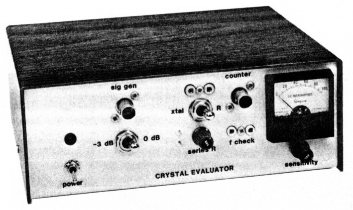
A tester for Crystal F, Q and R
This instrument allows you to analyze the crystals you want to use in IF ladder filters. The design is based on Wes Hayward's circuits in his classic QST ladder-filter paper.
Do you need a CW or SSB filter for a new project? Does the cost of commercial filters curl your hair? You can save dollars and design a filter for your needs by building this tester and following the instructions in Wes Hayward's QST articles on this subject.(1)
He described some circuits for crystal analysis in his 1982 article, but no PC-board patterns were offered and the practical data was not complete. I built two units that contained the circuits Hayward recommended, but I found them awkward to use because they weren't assembled for convenience. This third model puts all of the key circuits on one small PC board. I incorporated some circuit changes and added some features you should find useful.
Page space does not permit repeating the high points of the W7ZOI QST articles. Emphasis is on how to build and use this instrument. There is nothing tricky about the construction, and the cost is modest, especially if you have a reasonable supply of parts on hand.
Circuit notes
Fig 1 shows the circuit for the crystal evaluator. A 20-dB, 50Ω attenuator is used at the input port (J1). This helps to prevent the signal generator from overloading the broadband amplifiers, Q1 through Q4. It also provides a 50Ω input termination for the crystal under test. These considerations are important if we are to obtain accurate indications of the crystal characteristics. Q1 provides a 50-Ω load for the output of the crystal.
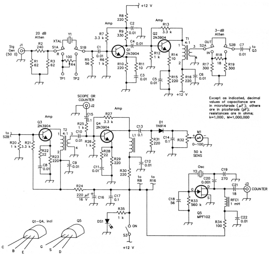
Fig 1 - Schematic diagram of the RF portion of the crystal tester. Capacitors are disc ceramic, 100 V. Those with polarity marked are electrolytic or tantalum. Fixed-value resistors are 1/4-W carbon composition.
| D1 | Small-signal diode, type 1N914. |
| DS1 | Red LED. |
| J1, J2, J3 | BNC chassis-mount connector. |
| L1 | RF choke. Use 15 turns of no. 26 enam wire on an Amidon Assoc FT-37-43 (850 µ) toroid. |
| M1 | Small dc meter, 100 or 200 µA (see text). |
| R4 | 100-Ω, linear-taper carbon-composition control. A 250-Ω control is also suitable. |
| R32 | 50-kΩ, linear-taper carbon-composition control. |
| RFC1 | Miniature 1-mH RF choke. |
| S1, S2 | DPDT toggle or slide switch. |
| T1, T2 | 4:1 broadband transformer. Use 12 primary turns of no. 26 enam wire on an Amidon FT-37-43 toroid. Secondary has 6 turns of no. 26 enam wire. |
| TP1, TP2 | Small press-in pin-type feed-through bushing or small binding post. |
| Y1, Y2 | Crystal to be tested. Use crystal socket of choice or parallel sockets for types of holders desired. |
I added S1 to permit switching between the crystal and R4. Originally, I had to plug the potentiometer into the crystal socket from outside the panel. TP 1 and TP2 are in parallel with R4 to allow resistance measurements from the front panel of the box. It is vital that the leads from the PC board to the Y1 socket, and from the board to R4, be kept very short. This minimizes stray inductance, which can cause improper readings, especially with crystals above 4 MHz.
Q1, Q2, Q3 and Q4 operate as broadband amplifiers. Total circuit gain is approximately 40 dB. A 3-dB attenuator is located immediately after Q2. The attenuator is switched in and out of the circuit by means of S2. Hayward provided a 3-dB gain reduction by changing the Q2 emitter components with a switch. I discovered that this approach could be tricky, depending upon the particular 2N3904 used. Some tailoring of values was necessary to ensure a 3-dB change. The resistive attenuator at S2 provides a dependable 3-dB drop in signal.
You can use a scope to measure changes in circuit response. J2 is provided for this purpose. If you choose this option, you can eliminate Q4 and the meter circuit. If Q4 is dropped from the circuit, terminate CIO (Q4 side) with a 56-0 resistor. You can attach a frequency counter to J2. Hayward connected his counter to J1, but I found that my counter was not sensitive enough to trigger at that circuit point. The counter works fine at J2 because of the amplification provided by Q1, Q2 and Q3.
Q4 functions as an amplifier for the metering circuit. D1 rectifies the RF energy to cause deflection of the needle of M1. R32 is a meter-sensitivity control.
I included the test oscillator, Q5, on the PC board. It is used for measuring crystal frequency via J3. This is essential when selecting closely matched crystals for a filter. Q5 functions as a Pierce oscillator. The feedback components (C18, C19) are suitable for I to 20-MHz crystals.
Construction information
Fig 2 shows the interior of the tester. The circuit is housed in a Ten-Tec TW-38 cabinet. It measures (HWD) 3-1/16 x 8-1/4 x 6-1/8 inches. There is a lot of unused space in the box. You may want to miniaturize your version of this tester by choosing a smaller enclosure. The power supply (see Fig 3) can be eliminated if you already have an outboard power source (12 V dc at 100 mA or greater).
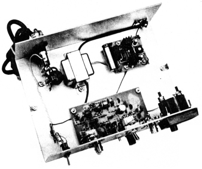
Fig 2 - Interior view of the tester. Note the RF PC board close to the front panel to ensure short leads to the panel hardware. J2 is on the rear panel. Terminal strips are used as tie points for the ac line and DS1. R35 of Fig 1 is mounted on one of the terminal strips.
The PC board is mounted on metal spacers near the front panel. It is situated for the shortest leads practicable between the board and the related panel hardware. RG-174 miniature coaxial cable is used between J1 and the board; likewise from J2 to the PC board. Ground the shield braid at each end of these cables.
I used a Simpson 100-µA meter for M1 of Fig 1. This is a high-priced component! You can use a low-cost edgewise surplus meter for M1. Most of these units have a 200-µA basic movement, and they are plenty sensitive enough for this circuit. Look for these S meters and battery indicators in the surplus catalogs. It is a simple matter to paste a homemade numbered meter scale over the original one. This will provide better reference marks when checking the -3-dB points of the crystal response.
T1 of Fig 3 is a surplus 12-V, 250-mA transformer. The output from the bridge rectifier, at the filter capacitor, is 16.9 V. A 12-V three-terminal regulator can be used in place of the LM3I7T variable regulator I use. Be sure to put a small heat sink on the voltage regulator, U2. My rectifier/ regulator module is a unit (modified) I ob tained from a surplus dealer. There is no PC pattern for this assembly.
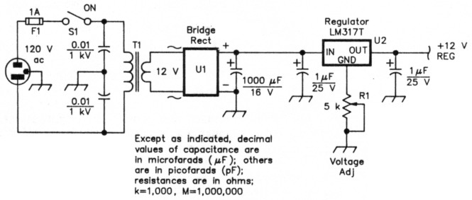
Fig 3 - Circuit of the 12-V power supply. Decimal-value capacitors are disc ceramic, 1 kV; those with polarity marked are electrolytic or tantalum.
| F1 | 1-A fuse in panel-mount holder. |
| R1 | Linear taper PC-mount control, 5 kΩ. |
| S1 | SPST toggle. |
| T1 | 12-V, 250-mA power transformer. |
| U1 | Bridge rectifier, 50 PRV, 1 A. |
| U2 | Adjustable voltage regulator or fixed-voltage unit (see text). |
The basics of tester use
Crystals used in ladder filters need to be matched within 100 Hz of one another - the closer the better, of course. Plug the crystal into the Y2 socket and attach a fre quency counter to J3. Select a set of crystals that is closely matched.
Next, insert one of the selected crystals into the Y1 socket. Connect a signal generator to J1 and place S1 in the XTAL position. Set S2 for 0 dB and set R32 at midrange. Carefully adjust the generator to the crystal frequency, as observed by a peak reading obtained on M 1. This is a touchy procedure, since you can pass across the crystal series-resonant frequency without seeing the needle of M 1 move! A generator with a vernier knob is essential for this test unless you are quite steady of hand. Note the frequency at which peak response occurs.
Now, switch in the 3-dB pad and log the meter reading. It will drop to the left. Remove the 3-dB pad and adjust the generator frequency above and below the crystal series-resonant frequency. Find the two points where M1 reads the same as with the 3-dB pad in the line. These are the 3-dB response points for the crystal. Use your frequency counter to measure the frequency at the 3-dB points. With this information you can determine the crystal Q, in accordance with the Hayward article referenced in Note 1.
The last procedure calls for relocating the crystal series-resonant frequency (maximum MI reading). Place SI in the R position and adjust R4 to obtain the same meter reading that was noted with Si in the XTAL mode. Now, measure the resistance of R4 across TPI and TP2. This provides the resistive characteristic of your crystal. This data is essential for designing your filter, as discussed in Hayward's article.
Use the lowest signal-generator output amplitude practicable, consistent with a midscale meter reading at crystal resonance. Feeding too much driving power into the tester will lead to inaccurate test results, and excessive drive can damage the crystal under test.
Some final remarks
I hope you will be encouraged to build your own crystal filters for transmitters and receivers. Certainly, the Hayward procedure is simple and easy to duplicate. The practical data for this tester is meant to stimulate you toward doing your own thing with crystal filters. Surplus computer crystals are widely available at low cost. Check the surplus catalogs for these units; most are in the $1 class.
Notes
- W. Hayward, W7ZOI, "A Unified Approach to the Design of Crystal Ladder Filters," QST, May 1982, p 21. Also see Hayward's "Designing and Building Simple Crystal Filters," QST, July 1987, p 24.
W1FB, Doug DeMaw.