Locking VCXOs to a GPS 1 pps Output
for the Microwave and mmWave Local Oscillators
Following previous articies where phase locking of VCXOs to a 10MHz stable reference were described, this article presents an implementation using the same hardware configured to lock to the l pps output of a GPS receiver. The circuit can be used to assure stability to microwave and millimeter-wave transverters without the need to maintain a high stability 10MHz reference, or simply to stabilize a 10MHz VCXO thus providing a secondary standard.
Introduction
The circuit described in this articie uses exactiy the same hardware as the previously published reference lock circuit(1) and universal phase lock(2) and consequently the same pcb and components, exception made for the resistors and capacitors forming the loop filter that should have their values adapted to this particular application and the coupling capacitors shortened on the reference input path to allow the 1 pps signal (TTL/CMOS) to pass through.
The circuit is built around an ALTERA device EPM3064ATC44-4 that is configured to implement a time lag phase comparator with PWM DAC output.
The device employed the EPM3064ATC44-4, (the -4 denotes 4 ns delay) can operate directly at above 180MHz of clock, being the actual maximum frequency dependent on the complexity of the circuit configured inside the CPLD. For this application nearly all resources of the CPLD were used being the actual limit around 150MHz therefore being useful to lock a VCXO safely up to 145MHz.
Circuit description
The circuit implements a phase comparator (phase/time lag counting method) and a PWM dac to output the result of the phase comparison. The phase comparison method consists in measuring the time lag between edges of the 1 pps signal and the scaled version of the signal to be locked. The VCXO signal is divided by a predefined value (set by the configuration input bits) to produce the required down scaled version of the VCXO. In this application is the VCXO that signal is used to clock most of the internal circuitry as the true reference signal. The l pps is too slow for that purpose.
At every l pps pulse the time lag value is latched providing a stable value throughout the entire 1 second period. This time lag value is continuously output to a 1 bit DAC using PWM.
Lock points
As the reference for the time lag measurement is the 1 pps signal, the time elapsed from the 1 pps to the other signal will be constant whenever this signal is an exact multiple of 1 Hz. This results in a similar scheme as in the universal lock version described in a previous article(2). The time lag increases if this frequency becomes lower than the exact 1 Hz multiple and decreases if the frequency becomes higher. The lock point becomes therefore the closest 1 Hz multiple. Therefore the actual lock points become 1 Hz multiplied by the VCXO division ratio set by the configuration table. The VCXO divider can be set to accommodate the convenient locking frequency least significant digits, however the values to be used must obey a criteria that ensures the time lag counter to reach the maximum dac value in order not to compromise the lock range. The internal sequencer uses a 2 bit counter that clocks the time lag counter at ¼ of the VCXO frequency so the main divider should provide a division by about 4 times the maximum time lag counter maximum in order to use the total DAC range. The lock points configured are presented in the table below, The values chosen should be suitable for most of the microwave local oscillator's VCXO.
- conf = 00 locks to 4 kHz multiples, best lock range, 10/100/96/90MHz etc.
- conf = 01 locks to 3 kHz multiples, 75% dac range
- conf = 10 locks to 2.5 kHz muitiples, 60% dac range
- conf = 11 locks to 2 kHz muitiples, 50% dac range, worst case.
Loop filter
The 1 Hz rate of change of the PWM-DAC suggests immediately that we must filter orders of magnitudes lower for correct averaging and insensitivity to the lpps signal jitter. This is absolutely right however we may be quite satisfied with the low jitter of the 1 pps that we can get from modern GPS cores and therefore only need to average the PWM frequency into a reasonably clean DC signal. The original values for the loop filter are enough to remove most of the PWM noise and can be used in this situation. lf some degree of averaging is however required you can simply scale both capacitors proportionally. Typical loop filter's R and C values to achieve some degree of averaging are: R1=100K R2=47K C1=1µF (stack two smd 470nF capacitors) C2=10µF(tantal).
Hardware changes
The 1 pps signal has aiready digital levels, presumably CMOS or TTL compatible, but it may be a good idea to buffer this before delivering it to the CPLD. The conditioning amplifier made using the two 74F04 inverters is no longer necessary for this 1 pps version, furthermore it is undesirable. The best way to solve this with minima] effort is to replace C3 and C4 by short circuits and not install R6 and R7. Also, as described previously, the loop filter must be set according to the rate of change of the PWM output signal and the VCXO tuning characteristics. No other hardware changes are necessary.
Conclusion
Locking to 1 pps gives you the uitimate accuracy with fuil mobility. The circuit can be also used at home to make a secondary 10MHz standard. Hardcopies of the PCB's at 4:1 scale, diagrams and ready to program *.pof files can be found at my web page: ???? Thanks to all for the support 1 received for these developments. This l pps version has some limitations regarding the possible lock point table changes. However, if you have any specific configuration need let me know by email and 1 will check if it fits inside the CPLD device.
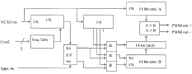
Fig. 1 - Block diagram of the logic implemented inside the EPM3064.
Sources
Several readers have asked for sources where to obtain the parts that were presented in the Microwave Parts column in the last DUBUS issues. Here we have some information.
Parts from Watkin Johnson can be obtained from:Fa. Richardson Electronics, Zeppelinstr. 2, D-82178 Puchheim.
Ansprechnpartner: Herr Guenter Hoffmann
T +4936781137090
F +4936781137099
E guenter@rell.com
Parts from RFMD can be obtained from:
Municom GmbH, Fuchsgrube 4, D-83278 Traunstein
T +4986116677-0
F +4986116677-88
I https://www.municom.de/de
References
- Locking VCXOs to 10 MHz for the Microwave and mmWave local oscillators. - L. Cupido - DUBUS 3 / 2002, p. 13.
- Locking VCXOs to 10 MHz, Universal Version and - L. Cupido - DUBUS 1 / 2003, p 15.
Luis Cupido, CT1DMK