Designing a station for the microwave bands 3
1296 MHz-10 GHz in one compact station
Part 1 discussed some of the advantages microwaves can have over lower frequency signals for point-to-point communications. I presented a generalized approach using phaselock techniques which allows access to the calling frequency on each Amateur microwave band and supports linear signal conversion: SSB, CW, and other narrowband modes. You can obtain a spectrally pure and precise local oscillator signal for any of the Amateur microwave bands with a single pc board design in several separate loops, including only those components needed for a particular loop. Table 1 in Part 1 showed that you can obtain SSB operation on all the Amateur bands from 1296-24192 MHz using a 1010-MHz reference oscillator to downconvert and phaselock an available microwave oscillator, along with an appropriate i-f and microwave signal mixer.
I've demonstrated this approach with the description of a 10368-MHz SSB station. But, its broader applications shouldn't be lost in the specifics of the 10-GHz example; the technique can be used with all of the microwave bands. You can achieve 1296-MHz, 2304-MHz, and 10368-MHz operation by adding the signal mixer/filters (a harmonic mixer with 1010-MHz LO drive can be used on 2304) once circuits for the 100-MHz quartz oscillator, 1010-MHz coaxial oscillator, and 10-GHz oscillator are functioning. Operation is possible at 3456 MHz and 5760 MHz with the addition of an oscillator/downconverter and signal mixer/filter. You can add more microwave amplification for transmit and receive on a band-by-band basis.
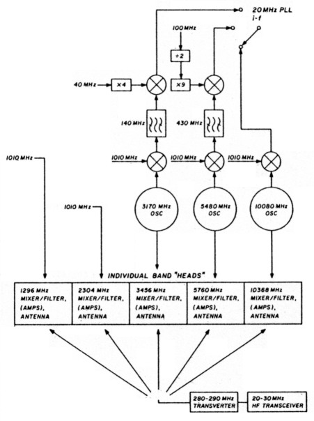
Fig. 1 - Once the 10368-MHz station using the 280-290 MHz signal i-f is built, 1296 and 2304 MHz are immediately available. The two microwave bands in between, 3456 and 5760 MHz, may be included by adding suitable VCOs at 3170 and 5480 MHz, along with harmonic mixers and circuitry to convert their PLL i-f to 20 MHz.
Although Table 1, part 1 showed how to get on all the bands using the 1010-MHz signal, some of the alternatives result in inverted tuning (high side LO) and a 432-MHz i-f. If you include a frequency conversion after the PLL harmonic downconverter, normal tuning and exclusive use of the 280-290 MHz i-f is feasible. Figure 1 shows the block diagram for a five-band LO. You don't need to construct additional phaselock circuitry; you can use the 10-GHz phaselocking circuits for multiple bands as long as you provide similar oscillator tuning sensitivities. To change bands, simply switch the power and PLL i-f to the desired oscillator/downconverter. Photo A shows a phaselocked transverter with provision for five bands, having little more circuit complexity or size than previous single-band units.
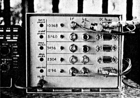
Photo A - Five-band operation is easily obtained using this phaselocked transverter.
You can get immediate 10368-MHz SSB operation if you have a 148-MHz transceiver and proper reference frequency to give a 10220-MHz LO. However, you'll need a 280-290 MHz i-f to take advantage of the potential multiband operation. Part 3 shows the circuits for the 260-MHz phaselocked oscillator, and the amplifier and switching circuits used to convert a 2030 MHz Amateur transceiver to and from the 280-290 MHz intermediate frequency required for multiband microwave operation. I'll also show the two-stage GaAsFET amplifier used for the 10368 station.
260-MHz local oscillator
I'll begin the description of 280-290 MHz transverter with the 260-MHz phaselocked LO. It would have been easy to use a conventional approach because this transverter isn't very different from a low power (zero dBm) 220-MHz one. I could have used an 86.666-MHz crystal oscillator followed by a tripler and appropriate filtering, but I didn't want to compromise the frequency accuracy of the microwave station with a less accurate unlocked i-f transverter LO. You can maintain overall frequency control by the 10-MHz frequency standard (or the 100-MHz crystal if it's operated unlocked) by using another common phaselock board and building a VCO at 260 MHz.
Obtain the 40-MHz PLL i-f by mixing the VCO output with the third harmonic of a 100-MHz reference signal. A standard double-balanced mixer (like an SRA-1) works well because it's effectively an odd harmonic mixer. A harmonic downconverter produces an appropriate i-f for locking. The oscillator uses a junction FET. (I make no claim that it's the best that can be done.) It isn't necessary to have superlative spectral purity in this application because, unlike the 1010-MHz case, no higher harmonics are used for further phaselocking; simplicity of design and ease of construction win. Even so, the spectrum of this LO when locked is good, and doesn't contribute significantly to microwave signal phase noise. The 260-MHz bandpass filters and buffer stages are present only for isolation and to keep any reference frequency derivatives from showing up on the 260-MHz signal. If you take care to separate the PLL i-f signals from the main 260-MHz output, any spurious signals are at least 75-dB down. Photo B shows the oscillator.
Photo B - This oscillator is used in obtaining the 260-MHz LO.
You'll need a 40-MHz reference frequency to lock this oscillator. A 20-MHz ECL reference signal drives a bipolar transistor frequency doubler, which drives an extra ECL line receiver. These circuits are located on the previously constructed 100-MHz reference board.
As with the 1010-MHz downconverter circuit, a 100-MHz bandpass filter and amplifier keeps any lower frequency signals on the ECL output from passing straight into the PLL i-f amplifiers through the harmonic mixer.
All of the locking circuits are identical to the ones used before. Table 2, part 1 shows component values for the loop filter. Component values for the lowpass filter after the harmonic mixer are modified to pass the 40-MHz PLL i-f. Use the jumpers marked "-" on the common phaselock board. Figure 2 shows the schematic of the oscillator/amplifier and PLL i-f. The 40-MHz reference circuit is shown in fig. 3. Figure 4 shows the spectrum of the phaselocked 260-MHz oscillator.
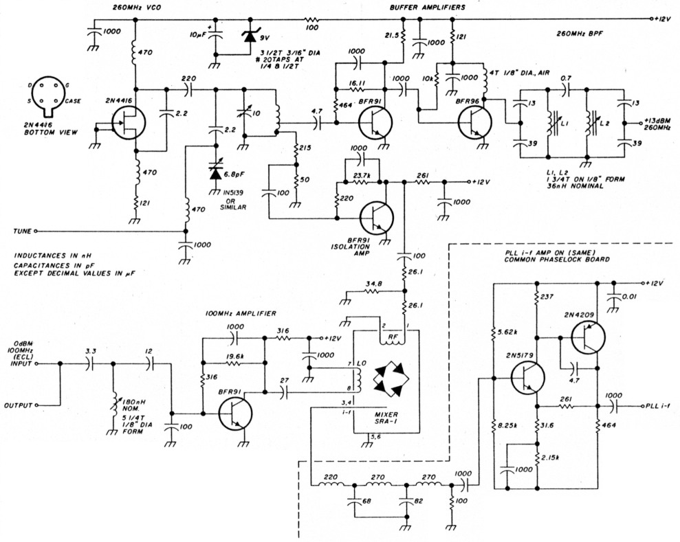
Fig. 2 - The 260-MHz phaselocked LO for the 280-290 MHz transverter uses a simple junction FET oscillator and two different amplifiers - one for the signal mixer and the other for driving the harmonic downconverter.
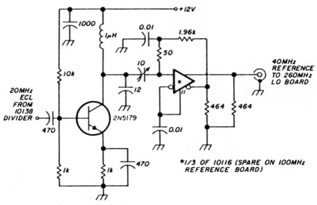
Fig. 3 - The 260-MHz locking circuitry requires a 40-MHz reference frequency. This is obtained by doubling the existing 20-MHz ECL signal in a transistor and restoring ECL logic levels with an extra 10116 line receiver.
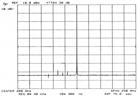
Fig. 4 - The spectrum resulting from phaselocking the 260-MHz VCO is quite clean. Both spurious signals and noise are small compared to the carrier.
280-290 MHz transverter mixer, amplifiers, and switching
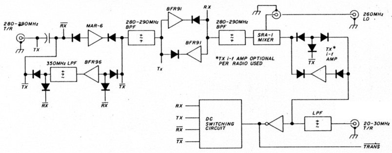
Fig 5 - The transverter uses a conventional double balanced mixer, broadband amplifiers, and appropriate filtering to convert the 20-30 MHz hf transceiver to 280-290 MHz. Transmit/receive switching is performed by PIN diodes and a dc switching circuit, which provides bias for the appropriate stages. Transmit output power of about 0 dBm (1 milliwatt) and receive conversion gain of about 8 dB is provided.
Figure 5 shows a block diagram for the 280-290 MHz transverter, fig. 6 is the schematic diagram and fig. 7 shows the dc biasing scheme. I tried to use easy to find parts and a design requiring a minimum of test equipment for final tuning. Broadband amplifiers are used in the hf and VHF portions of the transverter. Frequency selection is performed with a lowpass filter at hf and two 2-resonator filters for VHF. It's desirable to have a moderately high-gain low noise input stage to set the overall noise figure on receive at VHF. I chose an MMIC since Avantek/Mini Circuits MMICs seem to be easy to find at reasonable prices. I tried a MAR-8 (Avantek MSA-0885) first, and got good performance after taking care with grounding and construction techniques. To increase stability, I used a 30-ohm resistor in series with its output. The MAR-8 doesn't have heavy internal feedback to control its gain (and SWR), and provides a noise figure in the area of 3 dB. But this device is only conditionally stable and has lots of bandwidth - several GHz of it. You must control feedback paths as well as source and load impedances over a very large frequency range in order to keep it from oscillating. I replaced the MAR-8 with a MAR-6 (Avantek MSA-0685) and got a better match. The MAR-6 is unconditionally stable, with better input and output match. This is important because the 280-MHz filter, if not the microwave signal mixer, requires low SWR terminations for minimum ripple and insertion loss. However, the MAR-6 has lower gain at 280 MHz than the "resistor stabilized" MAR-8. This results in a 0-3 dB conversion gain for the transverter with the MAR-6, in contrast to about 8 dB with the MAR-8. The extra gain with the MAR-8 helps the noise figure by overcoming the 280-MHz filter losses and interstage amplifier noise figure. Measured overall, transverter noise figure is about 3 dB with the MAR-8 and 5 dB with the MAR-6. If you use signal frequency amplifiers, and not just a "barefoot mixer", the lower conversion gain and higher noise figure of the MAR-6 may not be a concern. If you choose a MAR-6, change the collector bias resistor to 390 ohms and remove the 30-ohm series resistor required for the MAR-8.
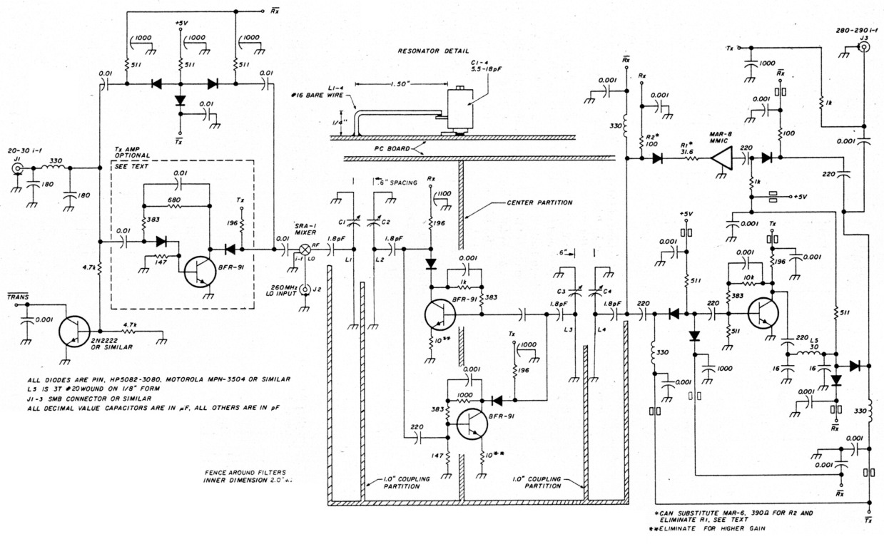
Fig 6 - Schematic of the 280-290 MHz transverter.
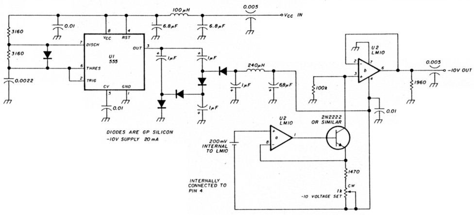
Fig 7 - DC biasing scheme for the 280-290 MHz transverter.
I use a BFR-96 on transmit, with the appropriate collector and feedback resistances, to provide a compromise of gain and match at 280-MHz. This stage only needs about zero-dBm output to drive the signal mixer (assuming microwave LO power in the + 10 dBm vicinity). The interstage amplifiers used between the two filter portions ensure a good input and output match for the filters to work against. I could have used a 4-resonatpr filter without interstage amplifiers instead of twin 2-resonator sections, but I felt that tuneup without test equipment would be harder. The mixer should probably look into a broadband 50-ohm termination instead of a filter for best signal performance and lowest conversion loss, but once again simplicity won out. Unwanted LO leakage and image signals should be at least 60-dB below maximum output. Figure 8 shows the output spectrum of the transverter on transmit.
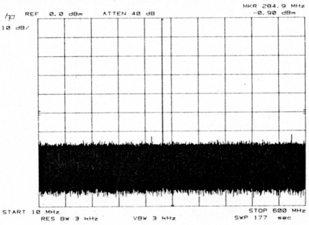
Fig 8 - The spectrum of this transverter on transmit shows unwanted signals suppressed by more than 60 dB. At full output of about 0 dBm only the 260-MHz LO feedthrough and the second harmonic of the signal are visible.
For transmitting, special circuit versatility is necessary in the transverter's hf circuit. This is because there's no standard transvert-mode output power level for modern multiband Amateur transceivers. Some manufacturers provide outputs of 1-100 milliwatts, while others are almost 30 dB less. I used another BFR-91 stage which can be "programmed" for various gains. The values on the schematic are right for my ICOM IC-751; it puts out about - 15-dBm maximum on SSB/CW transmit in transverter mode. If your exciter has more drive than this, you may need to eliminate the stage or put in a resistive attenuator. As shown, the transverter puts out about 0 to +3 dBm on voice peaks of my IC-751. The PIN diode switch lets the full mixer output reach the receiver during receive. If your station receiver has particularly low gain, you could include another amplifier stage here. This shouldn't be necessary for most applications using microwave preamplifiers. Even with a "barefoot mixer", the transverter as shown exhibits 8-10 dB conversion gain on receive. This should make up for most of the conversion loss from a microwave mixer.
The 280-290 MHz filter was designed to be easy to use and construct. The inductor is an extremely simple and reproducible wire-over-ground plane. I was concerned that most of the coupling between resonators might be between the tuning capacitors themselves, and too dependent upon construction technique and layout. However, construction with a number of different types of tuning capacitors produced similar results.
Other possibilities
Because this filter is the only block (besides the LO) which controls frequency, you should be able to obtain transverters for 144, 220, and 432 MHz by changing the filter elements. This might be attractive at 220 MHz as a frequency doubler driven by the 100-MHz reference could provide the LO. A 120-MHz phaselocked VCO with a 100-MHz downconverter reference and 20-MHz PLL i-f would work for 144 MHz. The downconverter could be a conventional mixer. A fourth-harmonic anti-parallel diode mixer with 100-MHz reference and 10-MHz PLL i-f would suffice to lock a 410-MHz VCO for 430-440 MHz operation.
Switching
Because of the number of possible bands, I devised a standard transmit/receive interface - each with its own microwave head (mixer, filter, amplifiers and T/R switch). You should get full microwave output power on transmit, with zero dBm of i-f power. I chose to use Vcc on the rf signal line to indicate transmit; this allows "daisy-chaining" control. When the hf transceiver signals transmit by pulling the NOT-transmit line low or putting Vcc on its signal line, the 280-MHz transverter amplifiers are turned on in the transmit direction, and Vcc is passed to its rf port. As a result, the connected microwave circuitry goes into transmit. For this reason, hardware for each microwave band can be located at, or near, the antenna, minimizing feedline losses. Any band can now be selected from the operating position by connecting the i-f from the transverter. The local oscillator signals incur power losses on the way to the heads. BLt, excess LO power is generally available and microwave signal mixer conversion efficiencies aren't much influenced by moderate reduction of LO drive, as long as LO power is several dB greater than the maximum i-f power of zero dBm. Even at 10 GHz where losses are greatest, you can probably locate the microwave head and antenna at least 10-20 feet from the operating position if you use good quality coax. All that's required between the operating position and the head for each band is the connection of two coaxial cables, i-f and LO, and one dc power cable (where needed). This allows for continuing enhancements in the microwave heads, improved noise figure, and higher power amplifiers - without the necessity of impacting the local oscillator sections. Feedhorn/head combinations can be quickly exchanged using a single antenna during a band-change, if you provide a mount for a standard box at the feedpoint of a reflector antenna.
Because the 280-MHz transverter is electronically switched, transmit turnaround time should be that of the hf transceiver alone - unless there is a slower mechanical T/R switch in the microwave head. Microwave AMTOR should work with this arrangement.
Although Vcc may be indicated as 12 volts on some of the previous schematics, I actually run the entire station from the output of a low-dropout 3-terminal adjustable regulator set to 11 volts. This tends to keep gains and amplitudes stable, and allows operation on nearly discharged 12-volt automotive batteries. A separate 5-volt regulator provides the power for the ECL logic.
Transverter construction
I built the 260-MHz VCO in the space on the common phaselock board allocated for the 100-MHz oscillator and divider circuits. Because the board was made with lots of component-side ground plane, I soldered right to the ground plane or mounted components by their leads. Lead length was kept to a minimum. To do this, use 1/8th or 1/16th-watt resistors, and other physically small components. (I find that a large pair of tweezers is a great construction aid.) The lower impedance of the broadband amplifier stages tends to make them less sensitive to parasitic capacitances, which can be layout and lead-length dependent. Be particularly careful to connect directly the ground end of the capacitors and the coils on the 260-MHz band-pass filter. A clean, phaselocked + 10 dBm 260-MHz signal results if the phaselock downconverter and 260-MHz amplifier/filter portions are kept at a reasonable distance from one another.
The 280-290 MHz circuits are built using a similar technique. But, for this board I started with a bare piece of approximately 3" x 6" double-clad 1/ 16th-inch thick FiberglasTM pc board material (G-10). I cut 0.100"square pads and soldered all rf components to the board instead of building much of the circuit above the ground plane, as I did with the 260-MHz oscillator. Cutting out pads is easier than it sounds. You can prepare the entire board in one sitting with a microscope. Use a small hobby knife to cut away the copper around the pads. You'll get an isolated pad by scoring through the copper, then shifting the blade and cutting a vee or trough into the top of the board around a 0.100"square. As with the 260-MHz oscillator, the small component and pad size force you to control and limit the lead length. All ground connections should first be drilled completely through the board in the MMIC area. Then solder the component or lead to be grounded on both the top and bottom, to reduce the possibility of coupling inside the board. I drilled holes to clear the packages of the MMIC and the output BFR-96 transistor. This let me solder the emitter leads to the topside ground without excess lead length. Drill a hole for these leads and solder them to the top and bottom ground planes.
Be sure to follow the dimensions when making the filter inductors and mounting the tuning capacitors. The spacing between resonators in each pair is important to set filter coupling and provide the correct 8-10 MHz bandwidth. After cutting the pads and building the interstage amplifiers, solder the pc board "fence" on both sides around the filter assembly. The hf circuitry isn't critical, but I used the same "mini-pad" technique. It's desirable to connect the 260-MHz LO signal to the mixer with a piece of small coax. Try to use coax with an 0.D. of 1/8" or smaller. Use minimum length on both the mixer and connector ends to avoid radiating 260-MHz energy around the filter, where it may be amplified during transmit by the output BFR-96. Such radiation could cause the unwanted LO feedthrough to be suppressed by less than 60 dB. This radiation would be in-band and small on all of the microwave bands, but it's unnecessary.
I built the dc switching circuits on a piece of breadboard, which I mounted at one end of the transverter. I suggest using a 0.125-A fuse or foldback current limiting in the dc supply until you've finished troubleshooting and tune-up because the PNP transistors will self-destruct if their cases, or the RX or TX supply lines are inadvertently shorted when they are turned on. In normal operation, all these transistors are used as switches and have very little power dissipated. I brought out the NOT-Transmit line to allow keying when an hf transceiver providing Vcc on the signal line during transmit is unavailable. This point may also be monitored to tell if the hf transceiver is successful in causing the microwave station to go into transmit mode.
260-MHz LO tune-up
Finish the 260-MHz LO first; you'll use it to make the 280-290 MHz circuits work. Check your wiring and measure the current to the oscillator and each amplifier stage individually. As with the other loops, the phaselock portion, from the bipolar i-f amplifier onwards, can be checked by substituting one of the previously completed loops. A moderately sensitive detector of 40-MHz energy is desirable to tune the downconverter. An oscilloscope or a 40-MHz receiver should work. If you have neither, tune the oscillator to 271 MHz by listening to the PLL i-f at 29 MHz with the station receiver, to the PLL i-f at 29 MHz and tuning the variable capacitor slowly through its range. Do this with 6 volts applied to the tuning input. Verify that the signal heard tunes with the correct sense, and that you aren't overloading the receiver. Once you hear a signal which tunes correctly, peak it by adjusting the 100-MHz bandpass filter. To verify that the 40-MHz reference signal is present, use the diode detector from part 2, an oscilloscope, or other detector. To maximize it, peak the bipolar frequency doubler's collector tuning. Once the reference and PLL i-f inputs on the ECL phase comparator are at the correct level, the loop should lock when the VCO is (reltuned to near 260 MHz. If you have trouble getting a sufficient level on the PLL i-f, temporarily bypass the attenuators on the input and output of the isolation amplifier to increase signal levels. It may be useful to count the VCO and keep track of operation during tune-up if a VHF frequency counter is available. Once the oscillator locks correctly with both isolation amplifier attenuators connected, peak the 260-MHz output by tuning L1 and L2 on the 260-MHz bandpass filter. You should now have a clean and accurate 260-MHz LO.
280-290 MHz tune-up
After completing rf circuit construction and rechecking the wiring, apply Vcc to each of the active stages with the switching circuitry disconnected. Measure and verify proper collector or emitter current. Verify that the TX, RX lines, and their complements alternate appropriately between nearly Vcc and ground as the TRANS line is alternately shorted to ground and allowed to float.
Once individual stage biases are correct and the switching circuits are functioning, complete the transverter construction by wiring the switched lines to the rf circuits. The transverter is probably best tuned on receive by using a local signal source in the 280-290 MHz range. The second harmonic of a 2-meter transceiver may be used, or the tenth of a 10-meter transmitter. Hook up the 260-MHz LO and the station receiver to the transverter. When you identify a suitable test signal, couple it to the bandpass filter nearest the interstage amplifiers on the MMIC side (280-MHz signal connector side). Tune the pair of resonators on the mixer side for maximum response. Next, couple the signal at the MMIC output side of the filter assembly and peak the other two resonators for maximum. The transverter should now be roughly tuned and operate on both receive and transmit. You can perform fine tuning to flatten the response over the full 10-MHz range by peaking one of the resonators in each pair on a 281-MHz signal and the other on a 289-MHz signal. If a 1290-1300 MHz transceiver is available, generate these i-f signals by connecting the 1010-MHz oscillator to a double-balanced mixer filter and completing the 1296-MHz station. The Mini-Circuits SBL-1X or TFM-2 mixers are only rated to 1 GHz for full specifications, but still perform reasonably well at 1296 MHz. If you use this method, you can tune up the transverter on either transmit or receive.
10-GHz amplifier
This two-stage amplifier was the next logical step in station improvement. Low noise amplificaticn ahead of the mixer is necessary to reduce the overall receiver noise figure on receive. Without it the noise figure is approximately: NFrx = NFif + CEmix (+ 3 dB).
Where:
NFrx = receiver noise figure in dB
NFif = 288-MHz i-f receiver noise figure in dB
CEmix = conversion loss of the microwave signal mixer.
Even with an amplifier you get the additional 3 dB because, unless an image reject signal mixer is used, the noise at the image frequency is converted to the i-f and degrades the overall noise figure. The system noise figure can be essentially that of the amplifier alone by providing sufficient gain ahead of a bandpass filter which passes only the signal frequency and not the image. On transmit it's desirable to have more power than the few hundred microwatts the mixer alone can achieve; gain is required to do this. Amplifier gain is worth more than low noise figure because it overcomes other hardware noise figure problems on receive, and directly adds to output power on transmit. This can mean 2-dB of station improvement for every extra dB of amplifier gain. For these reasons, the amplifier was designed to have a compromise of good noise figure and maximum gain.
Design considerations
Neither low noise or high gain are as easy to achieve at 10 GHz as at lower frequencies. Gallium Arsenide field-effect transistors are currently the most readily available and suitable devices. Recent volume production of 4-GHz TYRO equipment has helped reduce the price and improve the performance of these parts. Gain elements aren't the only problem - losses in all circuit components whether lumped (like chip capacitors), or distributed (like microstrip transmission lines), must be kept to a minimum. Another significant problem (though not as noticeable at lower frequencies) is radiation loss. Wires, lines, and connections are no longer small in terms of the signal wavelength. Unless you take care to avoid it, a circuit can look more like an antenna than an amplifier. Building a circuit on a 2-1/2" long circuit board at 10.368 GHz is comparable to building one on a full-size football field at 40 meters. Packaging circuits at these frequencies can be a challenge since cavities and resonances resulting from mechanical dimensions can cause unexpected results. Can you imagine connecting one end of a coupling capacitor to a goal post and the other to the 20-yard line?
I chose a NEC NE-710 for the input stage and a NE-720 (or 2SK571) for the second stage. The 710 has lower noise and higher gain, while the 720 is relatively inexpensive. The 2SK571, which may only be available in Japan, is a bargain at about 500 Yen ($4 US) on the surplus market there. The 710 is matched and biased for near minimum noise figure while the 720 is matched for maximum gain.
About 6 of these amplifiers have been built. Consistency has been good with "tuned" gain between 15.5-17 dB and noise figure between 2.6-2.9 dB at 10368 MHz, for the group.
Construction
Unless suitable microwave test equipment is available, you should construct this amplifier after a stable narrowband 10368-MHz station is on the air. Because it needs to be made carefully, the experience gained in getting the downconverter and signal mixers operational should be useful in completing this amplifier.
The first circuits were made by "cutting and peeling" the microstrip traces from a piece of woven double-clad 1/32" TFE (Telfon-Fiberglass-Epoxy) board material. Rogers Corporation Duroid with random fibers was used for the final version because it's somewhat more uniform than woven board material. The woven board material can have a slightly different dielectric constant and shouldn't be substituted for the Duroid.
Use the highest-quality 4.7-pF coupling capacitors, especially in the input stage. About 0.5-dB improvement in noise figure was obtained by changing to high-Q capacitors from run-of-the-mill ones.
Repeatable performance depends upon carefully controlled grounding and component mounting. This is particularly true relative to the transistors themselves. The transistor source leads are soldered to the circuit side ground trace, but front-to-back shorting wires right at the transistor package and plated-through grounding holes are present every 0.100" to maintain good grounding. Careful drilling and wire front-to-back connections should work if a plate-through pc board process isn't available. The "half-moon" radial transmission lines provide an easy way to match impedances and connect bias at the same time. The bias wire can be a resistor lead or small wire soldered right at the junction of the transmission line and the radial line. I put a ferrite bead, held in place by some silicone rubber, on each of these leads for insurance against lower frequency oscillations. The other end of these bias leads connects to its associated feedthrough capacitor. Position the beads away from the circuit board and near the feedthrough capacitors. A 5-volt zener is also connected to each of these capacitors inside the compartment for static and overvoltage protection.
Figure 9 shows the circuit diagram for the amplifier and bias supply. The bias supply (designed by Bob Dildine, W6SFH), provided negative gate bias for this amplifier and higher power transmit amplifiers during the 1987 10-GHz DX record attempts. The LM-10 allows good regulation without needing excess voltage and current to turn a zener diode on hard. Build this supply in a separate shielded enclosure. Use good quality bypass capacitors on the input and output lines to make sure no switching frequency signals get out and contaminate the rest of the station electronics.
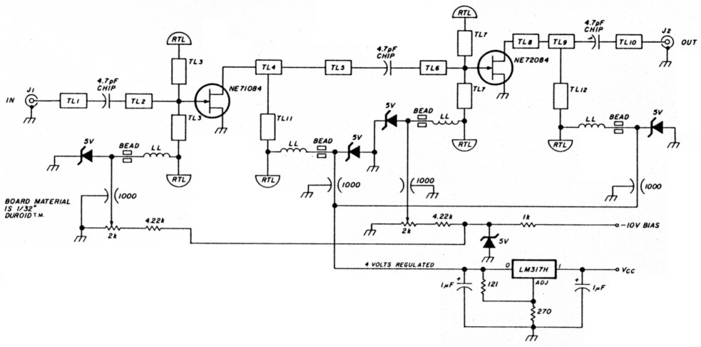
Fig 9 - The two-stage 10-GHz amplifier uses a low noise NE710 in the input stage followed by a less expensive NE720 in the second stage.
The SMA connectors flanges are soldered right to the board material on both top and ground plane sides. The notch in the board lets the face of the connector flange be flush with the edge of the board. The package is made from 0.030" copper sheeting cut to size, drilled for the feedthrough capacitors or connectors, and then soldered directly to the board as end and side walls. The package adds rigidity to the relatively flexible board material. Flexing can cause excessive strain and coupling capacitor breakage. Therefore, connector solder joints must be kept to a minimum. The SMA connectors are also soldered to the endwalls. Ground the gate and drain the circuits of both devices until you complete the assembly. Carefully assemble the transistors and coupling capacitors on the board with a microscope. Don't use a lot of solder. Take great care with these components; once they're soldered in place there is little chance of removing and reusing them. Interstage partitions can be made from 0.0050.010" brass shim stock. Notch them just enough to allow clearance for the transistor package and source leads. Carefully solder them in place after the side walls (with feedthrough capacitors and protection diodes) are on. The partitions should protrude about 0.100" above the sidewalls so that the covers can be soldered on after you complete the tune-up. The covers for the interstage and output should have 20-40 ferrite beads glued to their undersides. This suppresses package resonances which could degrade performance. The input compartment doesn't have these "absorbers" because any additional losses can degrade noise figure. Krazy GIueTM or similar contact adhesives seem to work and stand the temperature when the covers are finally solderedin place. Photos C and D show the completed amplifier with covers removed.
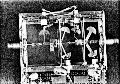
Photo C - The three compartments inside a completed amplifier are visible in this photograph. A shim "tuner" can be seen in the output stage (the largest compartment).
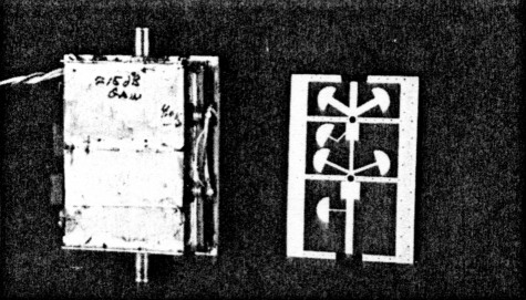
Photo D - This photograph shows the amplifier before and after the addition of the copper walls, connectors, and covers. Notches for the connector flanges and holes for the transistor packages are visible on the raw board.
Tune-up
You can do your tune up once the amplifier and bias circuits are completed, and either a station or other microwave test equipment is available. With the gate bias pots turned all the way down for zero-volts bias, gradually increase the drain supply voltage while watching the drain current. No more than 4.5-volts maximum should be necessary; going much beyond this will cause the protection zeners to start conducting. This zero-bias drain current, IDSS, varies from device to device; note the value for both stages. Next, slowly turn the bias pots to make the gates more negative. The drain current should diminish as you do this. Set the 710-bias current to approximately 25 percent of its IDSS value and the 720 to about 50 percent. You can adjust these later for minimum system noise figure if you have access to measuring equipment, but you should be able to obtain near optimum performance with these settings.
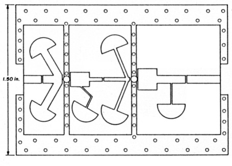
Fig 10A - The original pc board layout for the 10-GHz amplifier.
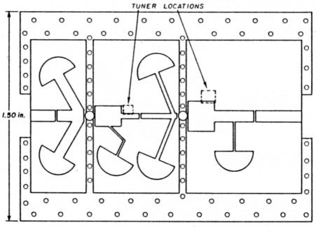
Fig. 10B - The pc board layout showing approximate placement of the tuning shims. Note: The shims are glued to the board after finding the exact placement.
An amplifier like this would require no tuning at lower frequencies. However, a little "tweaking" is useful at 10-GHz, as small variations in construction technique can affect performance. The need to adjust grew out of a mistake in the original design - that of not considering the extra circuit length provided by the gap over which the coupling capacitors are soldered. As a result of this error, untuned gain is about 13 dB. However, by adding small 0.05-0.100" square, 0.002" thick, brass shim stock tuners in the drain-matching circuits of the two stages, the amplifiers can be tuned for maximum gain. This also allows for small deviceto-device variations in the transistors. Figures 10A and B show approximate positions for the tuning shims. Tune by first gluing one of the shim tuners at right angles to the end of a toothpick. Carefully use the toothpick to move the shim around, varying the amount it extends past the edge of the transmission line, as well as its location along the length of the line. While you do this, monitor a stable signal on 10368 MHz with the station-receiver S meter. Be sure to maintain contact with the drain-circuit line of the stage. Note the optimum position, turn the power off, ground all bias pins to the amplifier, and permanently solder an identical shim in the position noted. You don't need to perform input-stage tuning because the match provided is not far off, even with the capacitor-gap error. As you can see in fig. 11, minimum noise figure occurs slightly above the hamband calling frequency - but the difference is negligible.
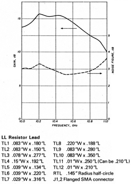
Fig 11 - The measured gain and noise figure of a typical amplifier. More than 15-dB gain and under 3-dB noise figure is readily available.
The finished amplifier should exhibit less than 3-dB noise figure and at least 15-dB of gain. On transmit it should be able to deliver 30 milliwatts of linear power and about 50 milliwatts saturated. You may need to increase drain current to more than 50 percent of the IDSS value for maximum output.
Summary
Once the 3456-MHz and 5760-MHz local oscillators are completed, further station improvements will come in the form of better receiver preamps and more transmit power for all the bands. I anticipate that the rapid bandswitch and good system modularity will provide a good contest station, as well as one which can grow with available technology. If you want to build a similar station and try for an obscure record, QSOs on 1618 different Amateur bands in 2-3 minutes should be possible with this equipment when augmented by a longwire antenna for the hf bands and standard VHF/UHF contest equipment. Another way to use this approach is for 900-MHz band operation. Use a 620-MHz VCO downconverted to a 20-MHz PLL i-f, with an anti-parallel diode mixer like the one used at 1010 MHz. This would give 900-910 MHz operation with the 280-290 MHz i-f.
I have ignored a couple of station components in this series. Transmit/receive switches are necessary in any station using signal frequency amplifiers. Many good units show up at flea markets and surplus stores. I also haven't provided construction information for a good ovenized frequency standard. Although the design presented here showed a 10-MHz standard, a good proportional oven around the unlocked 100-MHz oscillator may provide satisfactory results.
Thanks to Bob Dildine, W6SFH and Lynn Rhymes, WB7ABP for their interest, ideas, suggestions, and help with the station.
Part 1 - Part 2 - Part 3
N6GN, Glenn Elmore.