New thresholds in V.H.F. and U.H.F. reception; Circuit theory and diode details
Before getting into the thick of this month's installment it might be well to briefly review what has gone before in order to be sure what we're about. December QST showed something of the potential of new devices for v.h.f. and u.h.f. reception. January QST(1) discussed these devices with the emphasis on the reactance amplifier. It was shown that the important item in its operation is a voltage-tunable capacitor. It was also shown that under conditions of back-bias a semiconductor diode exhibits such a characteristic and should therefore be usable in this application. Now let us briefly rehash the basic circuitry in which this diode is to be used.
A brief refresher
Fig. 1 shows a simplified circuit which may be used for either frequency conversion or straight-through amplification. In this figure, tank 1 serves as an input tank to which a signal at a frequency fs is applied. When used as a frequency converter, tank 2 is tuned to the output frequency fo, which may be either higher than (up-converter) or lower than (down-converter) the signal frequency. The pump tank has only the job of providing an efficient means for exciting the diode capacitor at a pump frequency fp. The diode capacitor is represented in Fig. 1 by the strange-looking symbol. Pump and pump-frequency are nothing more than newfangled terms for a local oscillator and its output frequency. The pump performs a function similar to that of a high-frequency oscillator in an ordinary superheterodyne receiver.
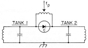
Fig. 1. Basic two-tank circuit.
When the circuit of Fig. 1 is employed as an up-converter, with the output frequency fo higher than fp (tank 2 tuned to fo = fp + fs), a stable power gain equal to fo may be realized with ideal diodes and lossless circuits. If the output tank is tuned to fp - fs, the gain relationship is -fo/fs. The negative sign implies that regeneration is involved and, depending on operating conditions, very high gains may be achieved.
When used as a down-converter, the output frequency is always lower than the signal frequency. For the case where the signal frequency is higher than the pump frequency, the gain is ideally fo/fs and since fo is smaller than fs we have a stable attenuator. Thus, if fo/fs is made small very high values of attenuation may be realized. Who knows, maybe someone can find a use for such a device. On the other hand, when fs is lower than fo, the gain is ideally fo/fs. Here also, fo is smaller than fs and the ratio fo/fs is less than unity. However, the actual gain for this arrangement, as in the case of the regenerative up-converter, may, in fact, be large if the device is adjusted to be highly regenerative.
It will be noted that for the regenerative arrangements fp is always the highest frequency in the system and is equal to fs + fp. In the regenerative condition the signal in tank 1 is amplified by the regenerative action and the device may be used as a straight-through amplifier merely by taking the output from tank 1 instead of from tank 2. The difference frequency fp - fs must, however, still appear in tank 2. The terms "idler" and "idler frequency" have become standard nomenclature for tank 2 and its frequency since they apparently have no purpose in life except that they must exist.
Two tank amplifier
A mild skirmish with the noise figure equations for the two-tank amplifier will be helpful in illustrating what's involved in designing and adjusting the devices for low noise figure. Fig. 2 shows a block diagram of the device and illustrates a way in which it might be used. The electrical circuit showing the principal elements which determine noise figure performance is given in Figure 3.
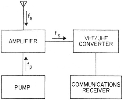
Fig. 2. A receiving system employing the two-tank amplifier.
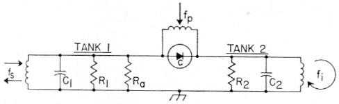
Fig. 3. Electrical circuit of the two-tank amplifier.
R1 is the shunt resistance representing the losses directly associated with tank 1, including losses in the semi-conductor capacitor (the shunt resistances representing the load and the antenna are not included).
R3 is the shunt resistance across tank 1 representing the antenna (or generator) resistance as transformed by the tuned circuit.
The theoretical noise figure of the two-tank amplifier has been developed in some detail by Heffner and Wade(2). For our purpose it may be represented to a good approximation by the relation:
![]()
The first term (unity) represents the thermal noise generated by an antenna (or signal generator) whose source resistance is at room temperature. The second term is the contribution added by the thermal noise associated with R1. The third term represents the thermal noise generated at the idler frequency in tank 2. This noise appears in tank 1 which serves as both an input and an output tank for the device. In this last term, the factor R is a shunt negative resistance determined by the operating conditions. If the device is giving a low noise figure with good gain, R will have a value only slightly greater than Ra and the ratio Ra/R can be omitted without much loss in accuracy. The equation then simplifies further to:
![]()
What does the equation tell us, having in mind our goal of having F as close to unity as possible? Since the first term represents noise which originates in the generator, we can't do anything about it. The remaining two terms when added together are a measure of the excess noise generated by the amplifier. Each of these terms should be kept as small as possible in order to keep their sum to a minimum. To minimize the second term we should couple the antenna tightly so that Ra is much less than R1. The third term may be made small by using an idler frequency much higher than the signal frequency. This means a still higher pump frequency, since fp = fs +fi.
Fig. 4 shows how the noise figure varies with pump frequency and different values of the ratio Ra/R1. The curve labeled Ra/R1 = 0 represents the best that can be accomplished. This is an idealized case in which R1 is considered to be infinitely large. This curve illustrates the importance of having a high pump frequency. For example, if a pump frequency equal to five times the signal frequency is used, the contribution from idler noise will be 0.25. The noise figure will be 1.25 (approximately 1 dB). In any practical circuit, however, the contribution from Ra/R1 will add to the 0.25 idler contribution with the result that the noise figure will be greater than 1.25. Thus, if you are straining for a one dB noise figure (F = 1.26) it would be more practical to use a pump frequency in the range of 7 to 10 times the signal frequency. The contribution from idler noise will then be in the range of 0.11 to 0.17. This would allow some room to maneuver in with respect to the contribution from R3/R1 which can then be in the range of 0.09 to 0.15 depending on the ratio fs/fi used.
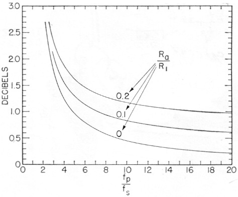
Fig. 4. Noise figure of the two-tank amplifier as a function of frequency and antenna loading.
Someone may be wondering about the noise associated with the load and whether it is amplified along with the signal by the regenerative action of the circuit. This matter is of some academic interest and is discussed in Appendix A.
Although the noise figure equation gives good directions on how to proceed, it does not tell the complete story. Nothing has been said so far as to how much capacitance variation is required from the diode capacitor and its pump. The required capacitance variation, ΔC, may be estimated from the relation
![]()
Here, QT1 and QT2 are the loaded Q's of tank 1 and tank 2 respectively. The loaded Q of tank 1 depends on Ra and R1, together with the effect of the actual load which for the two-tank amplifier will usually be a conventional v.h.f. or u.h.f. converter. In Fig. 3, R1 and R2 are shunt resistances representing the losses (excluding the effects of R3 and the load imposed on tank 1 by the converter) associated with tanks 1 and 2. For tank 1 the resistances R1 may be considered to be the parallel combination of a shunt resistance Rc1 resulting from the circuit losses of the tank itself and a shunt Rd1 representing the losses in the semiconductor capacitor at the signal frequency. A corresponding situation exists for tank 2. Note that only R1 enters directly into the noise figure equation but that both R1 and R2 are involved in QT1 and QT2.
The noise figure equation becomes complicated and somewhat sticky if the equation for the required capacitance variation is built directly into it. R1, C1, C2, ΔC and QT2 are all interrelated in a complex fashion which will be left as an exercise for the mathematically inclined. The end result, however, indicates that in order to minimize the noise figure of a practical device the following conditions are desirable:
- High idler and pump frequencies relative to the signal frequency,
- High-Q tanks,
- High Q in the semiconductor capacitor,
- d. A high available ΔC in the diode capacitor, and
- Small C1 and C2.
Other means for minimizing noise figure of the two-tank amplifier are available in addition to the suggestions given by the simplified equation. These are discussed in Appendix B as their application to amateur practice will probably be somewhat restricted.
The up-converter
The theoretical noise figure of the up-converter has been developed by Leenov.(3) The same general considerations such as high pump frequency and high-Q circuits and diodes that lead to low noise performance of the two-tank amplifier are also applicable to the up-converter. For this reason, the noise figure equation will not be given, although it is quite similar to that for the two-tank amplifier when translated into the same general form. The nonregenerative up-converter is attractive since it is stable and in practice will probably not require frequent retuning nearly as often as its regenerative cousins. Fig. 5 shows a practical configuration involving an up-converter and a crystal mixer in which the output appears at the signal frequency. This combination of up-converter and crystal mix r therefore performs the same function as a strait-through amplifier. It has the desirable feature permitting a self-controlled oscillator to be used for the pump without introducing frequency instability in the output. The configuration has one disadvantage in that the overall noise figure will be somewhat greater than that which can be obtained from a two-tank amplifier using the same diode and pump frequency. Fig. 6 gives the minimum noise figure which can be obtained from an up-converter followed by a crystal mixer with a noise figure of 4.8 db. The value of 4.8 db. is about as good as one can do with a conventional crystal mixer using currently available diodes designed for this purpose. Fig. 6 is based on the assumption that the thermal noise generated in the signal tank (tank 1) has been made negligible by extremely heavy antenna loading and is therefore an idealized case. The noise figure performance of the up-converter/crystal-mixer configuration as represented in Fig. 6 is therefore directly comparable with the idealized noise-figure performance of the two-tank amplifier as shown in the curve labeled Ra/R1 = 0 of Fig. 4.
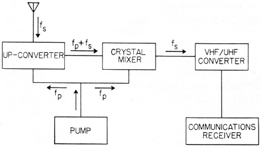
Fig. 5. A receiving system employing an up-converter and crystal mixer.
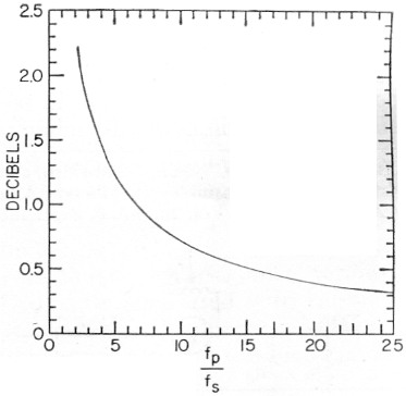
Fig. 6. Minimum noise figure of the up-converter/crystal mixer configuration.
The down converter
The regenerative down-converter arrangement illustrated in the block diagram of Fig. 7 is quite attractive from the point of view of the number of major components required for a complete receiving system. The noise figure equation is similar but not identical to that for the two-tank amplifier. In a simplified form it is given by the relation:
![]()
In this equation RL is the shunt resistance representing the losses introduced at the output frequency fo by the load. Typically, the load will be a communications receiver, as in Fig. 7. Inspection of the noise figure equation shows the principal difficulty in obtaining low-noise performance in the down-converter. Since fo is smaller than fa the ratio fa/fo may be quite large, as, for example, in a 144 Mc down-converter working into a 14 Mc communications receiver. In order to compensate for large values off it will be necessary to have extremely tight coupling between the load and the output tank. Existing diodes may not have sufficiently high values of ΔC and Q to give adequate regenerative gain with the heavy loading required for low-noise performance at low output frequencies. A further disadvantage of the down-converters is that very high regeneration will be required to give useful gains. When fo/fs is small a narrow bandwidth will result and the device will tend to have very poor gain stability. For these reasons down-converters with a high ratio off will probably be tricky to adjust and maintain.
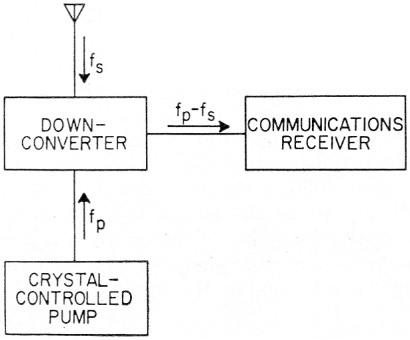
Fig. 7. A receiving system employing a down-converter.
Diode considerations
It has been shown that a back-biased semiconductor diode can provide the voltage-tunable capacitance that is necessary for the operation of reactance devices. Is the capacitive component the only one existing in such a diode? Unfortunately, no. There is some leakage across the dielectric which appears as a high shunting resistance. There is also some resistance in the mass of the material outside the depletion region which appears as a low series resistance. This series or spreading resistance is not the d.c. resistance determined simply by E/I in the forward direction. It is the dynamic or a.c. resistance in the forward direction, and is equal to the slope of the E/I curve after it has straightened out to be nearly linear. Rs is typically 0.25 to 2.5 ohms. Fig. 8 shows the equivalent circuit of the diode considering these three components, the small series resistance Rs, the large shunting or back resistance Rp, and the voltage sensitive capacitance, C. (Rp should not be confused with the RD1. mentioned earlier. RD1 is the shunt equivalent of the actual diode loss. Rp is of importance only at the lower frequencies.)
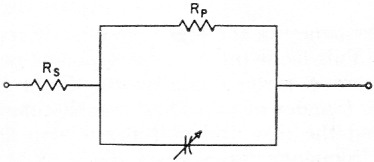
Fig. 8. Equivalent circuit of a semiconductor diode.
It is evident that resistive components are undesirable if the diode is to be used as the active element in a reactance amplifier. Resistance not only inhibits the gain of the device, but provides a source of noise. (Remember that a pure reactance cannot generate noise.) Therefore, in order to evaluate the usefulness of a diode for amplifier purposes, it is desirable to have a simple figure of merit based on these three characteristics. Such a factor turns out to be none other than "Q," the same as used for evaluating ordinary coils and capacitors which have reactive and resistive components.
Fig. 9 shows qualitative curves of the behavior of diode Q versus frequency for both germanium and silicon types. It will be noted that at the lower frequencies Q is dropping as it is limited by shunt resistance, hence the poor showing there by germanium, well known to be inferior to silicon in back resistance.
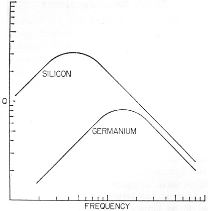
Fig. 9. Q vs frequency for representative silicon and germanium diodes.
At the higher frequencies, Q is largely limited by series, or forward resistance, and germanium does not make such a poor showing. For all practical amateur applications at the higher frequencies, the limiting factor will be series resistance and the quantitative expression for Q takes on quite a simple form:
![]()
From this, it can be seen why Q drops off linearly with frequency in the higher frequency region of Fig. 9. This leads one to expect poorer performance from a given diode as the frequency increases. (Shades of tubes and transit-time!) This is indeed the case and it is possible to define a cutoff frequency for a given diode as that frequency at which Q has dropped to unity, i. e., the resistive component is equal to the reactive. These cutoff frequencies typically fall high in the microwave region.
Maximizing diode Q
In order to maximize Q in a given diode, it is necessary to operate with as high a reactance as possible. This implies a low capacitance which in turn requires a high back bias. The limit to the amount of back bias that may be used is the peak inverse voltage (p.i.v.) of the diode. Beyond this value, avalanche breakdown may take place, the diode will begin conducting in the reverse direction, and a new shunting resistance will appear across the diode, deteriorating the Q. The behavior of the Q-versus-frequency curve for various levels of back bias is shown in Fig. 10 for a diode of 100-volt p.i.v. Note that in the high frequency region the Q increases with bias until the p.i.v. is reached and breakdown occurs. The Q then rapidly deteriorates, beginning at the low frequency end, due to the above-mentioned shunting resistance. It would appear then that for high-frequency operation we desire to operate as close to the p.i.v. as possible.
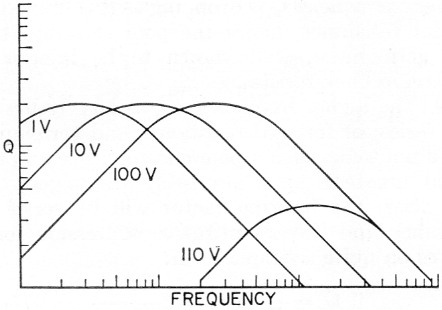
Fig. 10. Typical Q variation with frequency and bias for a diode having a peak inverse of 100 volts.
In what manner does the capacitance vary with the applied back-bias voltage? This is dependent on the junction structure employed. Where there is a sharp boundary between the p-type and the n-type material, the step or alloy junction shown in Fig. 11, the capacitance varies inversely as the square root of the bias. For what is known as a diffuse junction, see also Fig. 11, there is no sharp boundary between the materials, and capacitance is found to vary more nearly as the inverse cube root of the bias. Fig. 12 shows the variation of capacitance with bias voltage for a typical step-junction diode with a 50 volt p.i.v. The curve follows the expected V-½ law quite closely except in the region below 1 volt. The cause of the flattening of the curve in this region is the presence of a small constant "built-in" voltage in addition to the applied bias. This is the contact potential existing between the two dissimilar substances, the p-type and n-type material. Its magnitude is about 0.7 v. and it sets the practical upper limit on the diode capacitance. The V-½ law proves to be quite accurate when this effect is included. Another effect that may be observed in practical cases is an apparent flattening of the curve at the low capacitance end. This is due simply to the fixed static capacitance of the diode cartridge and may be considered to set the lower limit of available capacitance for cases not limited by p.i.v. Its value ranges from 0.1 pF for sub-miniature glass diodes to 0.4 pF for the microwave ceramic structure.
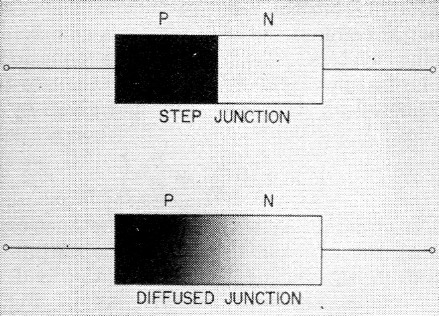
Fig. 11. Step junction and diffuse junction diodes.
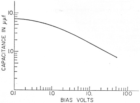
Fig. 12. Diode capacitance variation with back-bias voltage for a step-junction diode having a peak inverse of 50 volts.
It has been seen that Q represents a rough figure of merit by which diodes may be evaluated. It has also been seen that diodes may be classed in four different groups, germanium or silicon, each in either a step-junction or a diffused-junction configuration. Let us briefly consider the comparison of these four types on the basis of their theoretical Q's. An excellent discussion of diode Q is given by Spector(4), which indicates that in general silicon should prove superior to germanium, and that diffused structures should have an edge over step junctions. It is also indicated as a result of this theory that low p.i.v. diodes should be preferable. Experimental results concerning these considerations will be discussed shortly. It might be mentioned at this time that no improvement in overall Q is to be expected by either series or parallel operation of diodes.
Practical diode results
Evaluating presently available diodes for use in reactance devices is a fertile field indeed. The latest tabulation shows a total of over 2500 different semiconductor diode types. It has of course not been possible to test even a significant portion of this total and a certain amount of educated (?) guessing has been involved in selecting types to measure. For this reason the data contained here are not intended to be all inclusive but rather to serve as an indication of what directions might prove fruitful for future work.
A word or two might be in order about the methods of measurement involved in the determination of Q. Two methods have been used. The first is to use the diode in question to resonate a tuned circuit whose resonant impedance may be determined. This resonant impedance is then compared with that observed when an air capacitor of known Q is used in the same circuit. The second method is by use of a standard Q-meter, with the diode resonating a tuned circuit of known Q. When using this method, care must be taken to see that the r.f. voltage developed by the Q-meter is not sufficient to swing the operating point of the diode. Frequencies at which Q measurements have been made include 30, 50, 100, and 200 Mc., with the majority being made at 50 and 200 Mc.
Results of Q measurements of most interest are summarized in Table 1. Values of Qmax p.i.v. and C are given for those diodes which appear satisfactory for low-noise v.h.f. and u.h.f. use. The Q given is for the maximum bias condition, with the spread in Q being given where. available. The value of diode capacitance is a typical value that might be expected at ½ p.i.v. (½ p.i.v. might be considered the nominal operating bias if the maximum pump voltage is to be used to swing from zero volts to full p.i.v.) The manufacturer of each diode type is also given. The retail price of these diodes is $6.00 or less, with the exception of the MA-460A which currently sells for about $50.00. The 1N663 and the 1N660 are available from supply houses such as Allied Radio. It might be noted that the MA-460 series, designed specifically for voltage-tunable reactance use, should soon be available in improved versions such as the MA-460E with Q's of 300 at 200 Mc.
| Type | Q max at 200 Mc | P.I.V. | C at ½ P.I.V. | Manufacturer |
|---|---|---|---|---|
| 1N663... | 40-63 | 100 V | 2.0 pF | Pacific Semicond. |
| 1N252... | 51 | 20 V | 0.5 pF | Transitron |
| S266G... | 55 | 8 V | 0.5 pF | Transitron |
| DR303... | 112-122 | 75 V | 0.25 pF | Radio Receptor |
| 1N660... | 31-59 | 100 V | 2.0 pF | Texas Instr. |
| PS705... | 34-56 | 200 V | 1.4 pF | Pacific Semicond. |
| MA460A... | 115 | 9 V | 2.0 pF Microwave Assoc. | |
| 1N308... | 82 | 8 V | 0.3 55f | Raytheon |
Appendix C gives a list of marginal and submarginal diode types tested. The 1N21 and 1N23 series are conspicuous by their absence from any of the lists. Small but measurable Q's could be determined for these diodes but with no tunability. Point-contact silicon diodes do not appear suitable for reactance use.
Theory and results
Now let us consider briefly the overall results of the measurement program in the light of what was predicted theoretically. The diffused structures have indeed shown a superiority over the step junctions as to Q. However, it is possible that the greater tuning ratio of the step junction may partially offset this in practical use. The superiority of silicon over germanium has not been clearcut. The usefulness of silicon has been fully established but the situation for germanium has not yet been fully resolved because of the measurement difficulties resulting from the extremely small junction capacitances.
The theoretical prediction that low p.i.v. diodes would prove superior has not been verified. In fact, the indication has been that the high p.i.v. units have a slight advantage. This may result from the fact that the theoretical predictions assume comparison of a low p.i.v. diode designed to be a low p.i.v. diode, with a high p.i.v. unit designed to be high p.i.v. In the practical case of mass-produced diodes, junction design may well be aimed toward optimizing high p.i.v. characteristics, with those units failing to meet the spec being marketed as low p.i.v. That is, the low p.i.v. diodes are imperfect high p.i.v. design rather than optimum low p.i.v. design.
It is of interest to compare the measured values of Q with those computed on the basis of measured spreading resistance and reactance. The realized Q has been found to fall considerably short of the calculated values particularly for germanium and alloyed-silicon units. Diffused silicon junction units designed for fast recovery time show somewhat better agreement but still indicate that existing theory is not complete.
In outlining in general the diode characteristics that appear to correlate with high Q for use in reactance devices, it appears that the fast-recovery silicon diffused computer diodes, and extremely high forward conductances diodes of all types, hold the most promise. The higher p.i.v. units appear somewhat preferable. One precaution in considering high conductance units: rectifier types, even diffused, seem to have poor Q even though their forward conductance may be phenomenal. Their forward characteristic is due principly to a large junction area, a process equivalent to paralleling diodes, which is known not to increase the Q.
Diode Q and noise figure
It might be of interest at this time to attempt to determine what noise figures may be expected using a diode of given Q. Noise figure, however, is indirectly dependent on the ratio of tunable to fixed capacitance ΔC/C as well as being directly dependent on diode Q. Thus a fully rigorous figure of merit for diodes should include the effects of both Q and ΔC/C.
Fortunately the range of variation in ΔC/C between diodes is not nearly so large as the range of Q's encountered; in fact, for diodes of interest it differs by not more than 2:1. Therefore, it appears that we may solve the noise figure equations using a mean value of ΔC/C to determine a required Q, and state that practical Q's will vary about this value over a 2:1 range. This allows us to include the effects of ΔC/C without having to solve for each individual diode.
Table 2, then, gives the range of Q, as measured at 200 Mc, that appears necessary on the above basis to obtain the noise figure given. Note that the required Q ranges given are at 200 Mc so they may be compared directly with the mess:" ured values given in Table 1. In considering the values in Table 2 it might be noted that the low p.i.v. diodes and the germanium units would tend to require Q values at the high end of the range. For the high p.i.v. diodes the lower values of Q would be expected to be satisfactory.
| NF | 1 dB | 2 dB | 3 dB |
|---|---|---|---|
| fp/fs | 9 | 4 | 3 |
| 144 Mc | 18-36 | 7.5-15 | 4.5-9 |
| 220 Mc | 27.5-55 | 11.5-23 | 6.9-13.8 |
| 432 Mc | 54-108 | 22.5-45 | 13.5-27 |
| 1300 Mc | 162-216 | 67.5-135 | 40.5-81 |
The noise figures of Table 2 are theoretical and are based on certain assumptions, such as equal noise contribution from the idler tank and the diode, zero signal-tank loss, and a specified ratio of pump to signal frequency. Hams have been in this business long enough to know that theory is good only so long as it agrees with the results. How well these numbers agree will be determined in the next year or so as these devices are put to use. With the best available diodes noise figures of 1 dB appear attainable up to 432 Mc, and 2 dB at 1300 Mc
A discussion of experimental results and hardware details is planned for a future article. In the meantime there are no good reasons why a stock of the hotter diodes should not be laid in and experimental work begun.
Appendix A
Thermal and excess noise generated by the load affects the overall noise performance in a rather tricky way. Although the noise figure equation is correct, it tells us only how to minimize the noise figure of the two-tank amplifier. It says nothing about the coupling between the two-tank amplifier and the converter. As an indication of the difficulties which may arise, the ncise figure of the receiving system will be greater than that of the converter alone, if the converter is matched to the generator impedance and connected in parallel with the generator. Low receiving system noise figure will be obtained when the load is lightly coupled to the twc-tank amplifier. This, however, results in a higher gain requirement, narrower bandwidth and poorer gain stability of the device.
These problems can be avoided by using an esoteric device called a circulator. Circulators have a unique property of permitting power to flow in only one direction between certain pairs of terminals. By properly connecting a circulator in a receiving system, the noise generated by the load can be made harmless by dissipating it in a resistive termination. Unfortunately, these devices are available only for frequencies above 1000 Mc and have not yet appeared on the surplus market.
Another approach involves the use of two of the two-tank amplifiers connected in a receiving system in such a way that the load noise is cancelled out. If the reader is interested in pursuing this matter further, the technique is described by S. H. Autler, in connection with a similar problem involving masers, in the Correspondence Section of the Proceedings of the I.R.E. for November, 1958.
Appendix B
Thermal noise generated in the tanks and in the diode is directly proportional to their absolute temperature in degrees Kelvin. Noise figure might be reduced by immersing and keeping these components in a bath of liquid air or liquid nitrogen. This technique could be quite effective, but how you do this is your problem.
A second way to reduce noise figure is to terminate the idler tank in a separate directive antenna pointing at a cold spot in the sky. The region in the general direction of Polaris (the North Pole Star) is relatively quiet, permits a fixed antenna, and appeals suitable for the purpose. This method is not without its drawbacks. Idler frequency signals received by the idler antenna will be converted to signal frequency and appear in the output as interference. Also, the FCC has not yet seen fit to allocate "idler dumping" frequencies in which no transmissions may be made!
Appendix C
Measurements indicate that the following diode types are either not useful or of marginal value for use in v.h.f. reactance devices. They are listed so that further testing or experimentation will not be required to establish their merits for this application. All of these types did, however, exhibit variable reactance and might be useful at lower frequencies.
| Not Usable at V.H.F. | Usable but marginal | |
|---|---|---|
| S10G | 1N645 | DR670 |
| 1N482B | 1N91 | 1N283 |
| 1N484A | 1N674 | 1N270 |
| SG213 | TI600 | 1N279 |
| 1N461A | TI601 | S131 |
| HC7001 | TI604 | 1N659 |
| V27 | TI610 | 1N661 |
| 1N1252 | 1N145 | 1N643 |
| CK851 | 1N34 | PS700 |
| TI9G | PS703 | |
Notes
- Bateman and Bain, "New thresholds in VHF and UHF reception; Devices and diodes," QST, Jan. 1959.
- H. Heffner and G. Wade, "Gain, bandwidth, and noise characteristics of the variable parameter amplifier" Journal of Applied Physics, Vol. 29, No. 9, Sept. 1958.
- D. Leenov, "Gain and noise figure of a variable capacitance up-converter," Bell System Technical Journal, Vol. 37, July, 1958.
- C. J. Spector, " A Design Theory for the High Frequency p-n Junction Variable Capacitor," paper presented at the 1958 Electron Devices Meeting, PGED-IRE, Washington, D. C., Oct. 30-31, 1958.
Ros Bateman, W4AO
Walter F. Bain, W4LTU.