Key components of modern receiver design 2
First-IF AGC, a high-dynamic-range mixer, a low-noise VCO - here are circuits you may see "pretty soon now" in commercial gear. Or maybe you'll just build them yourself!
Part 1 of this article conveyed dynamic range, AGC and synthesizer concepts important in high-performance MF/HF reception. This month, we get down to putting these ideas into practice.
Building these concepts into a receiver
Achieving electronically controllable front-end attenuation is the first important step, and a conventional PIN-diode attenuator can provide it. The standard constant-impedance T PIN attenuator exhibits inter-modulation that increases with attenuation from 0 to -6 dB and then diminishes. To maintain a third-order intercept point of +30 dBm at frequencies above 1.5 MHz, a slightly different biasing scheme must be provided. Figure 6 shows a schematic of a suitable PIN-diode attenuator. These PIN diodes are not immune to second-order IMD on large signals, and therefore a preselector should be used in front of this AGC stage.
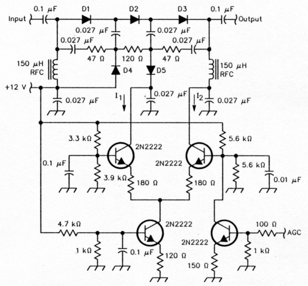
Figure 6-PIN-diode attenuator with dc amplifier for use in a high-performance communications receiver. D1 through D5 are Hewlett-Packard HP8052-3081 PIN diodes. The circuit's attenuation increases with increasing positive voltage at AGC.
In the IF, a differential amplifier with RF feedback as previously published in QST(6) should be used. Figure 7 shows this stage with an added overload-detection stage and first-IF AGC. The gain-controlled stage includes an AND function for local (AGC1) and global (AGC2) AGC. Figure 8 graphs the computer-simulated performance of a combination Norton feedback amplifier and differential amplifier as implemented by the BRF96-BFR96-BFT66 trio in Figure 7. It provides a noise figure in the vicinity of 2 dB and a high intercept point with very little reverse feedback. By contrast, the standard feedback amplifier often used in the post-mixer position suffers from unacceptably high feedback and is therefore frequently used with a small attenuator (commonly 6 dB) between its output and the crystal filter that follows it.
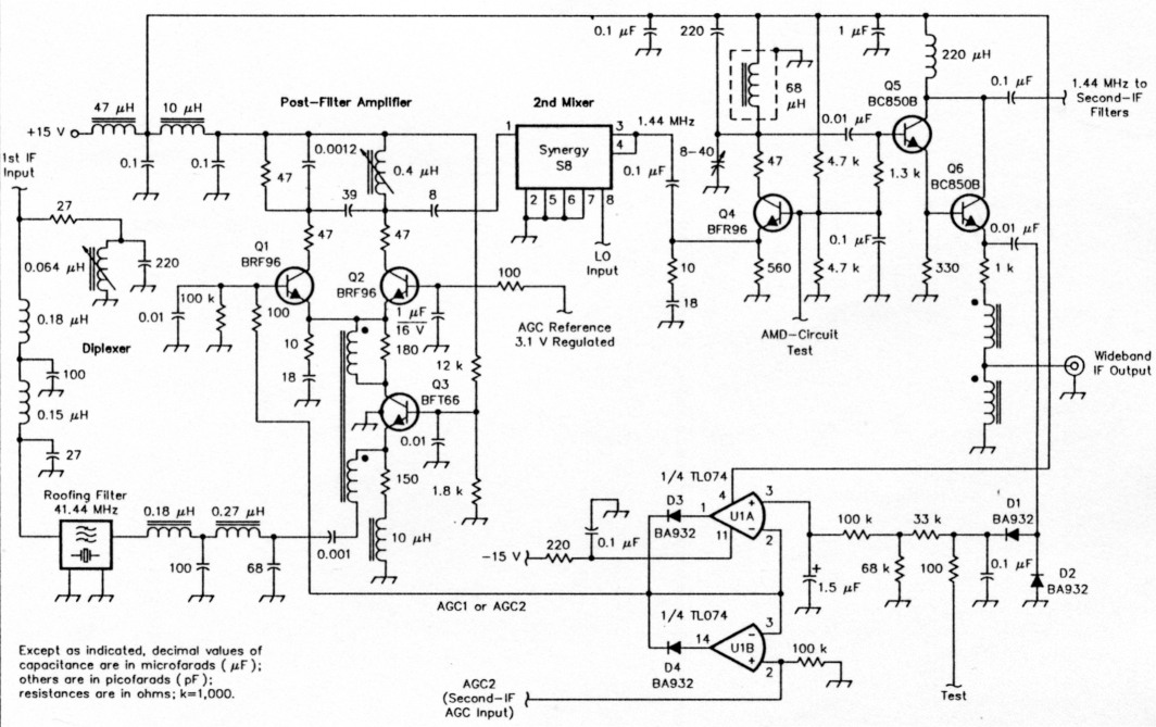
Figure 7-AGC amplifier and overload monitor schematic for a high-performance shortwave receiver. 01 to Q3 serve as a differential, gain-controlled post-roofing-filter amplifier. 04 acts as a buffer amplifier, Q5 drives the receiver's second IF stages (1.44 MHz), and 06 drives the AGC1 voltage-doubler detector (D1 and D2) and a wideband IF output. 01 receives control voltage via U1A (AGC1, the control voltage generated by detector/voltage doubler 01 and D2) and U1B (AGC2, the control signal generated by the receiver's second-IF AGC system).
The dual-AGC circuit acts as follows: The overload-control loop (AGC 1) is normally inactive, and the differential amplifier acts as part of the regular (AGC 2) AGC loop. When a strong signal falls into the window outside the second-IF filter and inside the roofing filter, the AGC2 loop does not respond to it. Instead, the ACC! loop applies a control voltage to the local AGC1controlled stage (Q I in Figure 7) and reduces its gain to prevent second-mixer overload.
The AGC1 loop protects the second mixer, bill what about the input of the AGCI-controlled amplifier itself? We can keep this circuit from being overdriven by activating the system's continuously adjustable front-end attenuator, which is included in the loop.
This three-loop AGC control system is currently the best possible way to deal with the real-world effects of finite intercept point in the various components in the chain. This approach is more costly than simpler systems, however, and thus is infrequently incorporated even in high-end military and commercial gear.
A key issue in the multiple-ACC-loop approach is the selection of the right AGC distribution and time constants. The best paper I've seen on this subject was published by J. Porter(7) but the sources cited in the references (see Part 1) should also be investigated.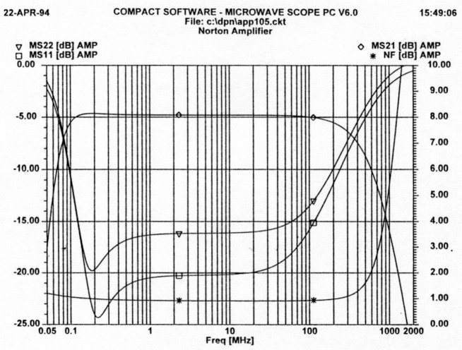
Figure 8-Performance of a combination differential amplifier and Norton noiseless-feedback amplifier as simulated by Compact Software's SCOPE 6.0.
Where to Put the Roofing Filter
Selectivity should he as high as possible as close as possible to the antenna, of course, but doing so can involve compromise. The system of which Figure 7 is part positions the first-1F crystal filter directly after the first mixer (see the block diagram in Figure 4). This is a compromise that causes two problems. One is that a crystal filter's input and output impedances are usually profoundly reactive within and adjacent to its passband, and mixers react violently to reactive terminations. The second problem is that filters are lossy, and this loss directly degrades the system's noise figure if an intermediate amplifier is not present to overcome it.
Traditional monolithic crystal filters exhibiting reasonable bandwidths of 15 kHz or less have input and output impedances from 600 to 1500 Ω. By the time two or three such filters are cascaded to obtain a reasonable shape factor, their combined loss can reach 6 to 8 dB. Adding the mixer loss (6 dB), the roofing-filter loss (8 dB) and the 4 or 5-dB noise figure of the traditional first-IF input stage results in an unacceptably high noise figure of 18 to 20 dB! The only recourse for a designer is to insert a postmixer preamplifier, which violates the concept of keeping high selectivity as close as possible to the antenna.
To avoid the necessity for a post-mixer amplifier, one must invest somewhat more money in a discrete-crystal roofing filter with an insertion loss under 5 dB (typically 3.5 dB) and follow it with a post-filter amplifier with a noise figure of 2 dB or less. This approach can provide a total NF of less than 12 dB-equivalent to 0.3 µV for 10 dB (S+N)/N with a bandwidth of 2.4 kHz. I implemented this post-mixer filter arrangement in the 1973-vintage SE 6861/11 ManPack by AEG Telefunken. Sabin independently published an excellent paper on the concept in 1981.(8)
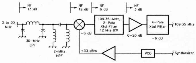
Figure 9-A high-performance receiver front end as outlined by Sabin (see Note 8). This approach uses two crystal filters to achieve an acceptable shape factor.
Figure 9 shows a high-performance receiver front end as outlined by Sabin. This approach resorts to two crystal filters, a two-pole and a four-pole, because its four-pole filter alone would be insufficiently selective. The amplifier between the filters is necessary because the four-pole filter has an insertion loss of 6 dB. Figure 10 shows a more modern approach that combines the techniques previously outlined. It uses one crystal filter that achieves the desired shape factor with less than 4 dB of insertion loss.
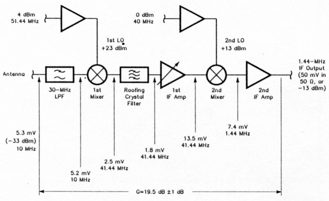
Figure 10-Level block diagram of the input stages of a modern, high-performance shortwave receiver. Note that the first IF amplifier in this system receives AGC, while the first IF amplifier in Sabin's paper (see Note 8) operates at constant gain. A practical system requires the addition of an RF preselector, which can be a set of sub-octave filters, a motor-driven multistage circuit or a binary-coded input filter.
How About Mixers?
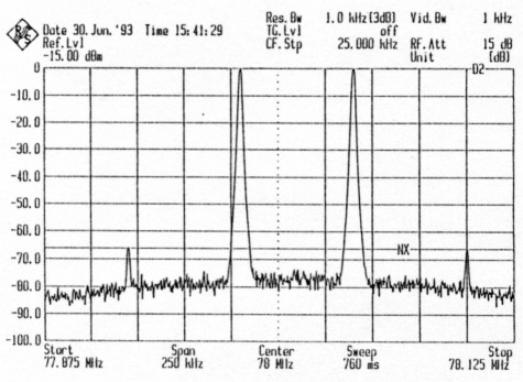
Figure 11-Result of a two-tone mixer test with 5-dBm tones at the mixer input. The two smaller pips are third-order IMD products.
The area of mixers, specifically switching mixers, has already received ample coverage. Figure 11 shows the result of a two-tone test of a mixer with 5-dBm tones applied to the mixer input. Figure 12 shows the results of a three-tone test using the same tone levels. To protect the spectrum analyzer, an external pad was added. Notice that the IMD product levels are pretty much the same in both cases, but that the number of spurious products significantly increases in the three-tone test.
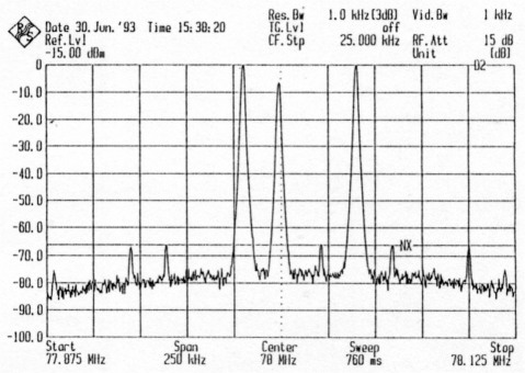
Figure 12-Result of a three-tone mixer test with 5-dBm tones at the mixer input. Additional third-order IMO products have appeared, along with the two-tone products shown in Figure 11.
Three-tone testing is a worthwhile extension of the two-tone testing with which radio amateurs are already familiar.(9) In on-the-air operation, the appearance of another strong signal between two strong carriers can be particularly annoying because of the significantly higher number of spurs generated. Three-tone testing can shed more light on a VHF or UHF radio's tendency to generate spurs in response to the many high-level VHF and UHF signals that exist in major metropolitan areas. Three-tone testing is also important because it can indirectly show a mixer's tendency toward cross-modulation. The transfer of modulation from a strong modulated carrier to weak unmodulated carriers is still observed on ham bands adjacent to or containing strong broadcast signals.
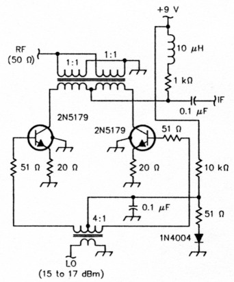
Figure 13-This single-balanced, push-pull transistor mixer achieves a high dynamic range (IP3 ≈ 33 dBm) with 15 to 17 dBm of LO drive. Its insertion loss is approximately 6 dB-comparable to a diode-ring mixer. A diode-ring mixer would require 25 to 27 dBm of LO drive to achieve the same IP3.
Recent mixer studies have lead to the development of a medium-frequency mixer that is well-suited to shortwave applications and home-built projects. Shown in Figure 13, it consists of two transistors in a push-pull configuration that is singly rather than doubly balanced. Because of the degenerative feedback introduced by the 2042 emitter resistors, the two transistors do not have to be matched. This mixer's real advantage lies in its achievement of a 33-dBm output intercept with only 17 dBm of LO drive. Typically, a diode ring with the same intermod performance requires 25 to 27 dBm of LO drive.
Tests indicate that the upper frequency limit of this mixer lies in the 500-MHz region. The circuit's lower frequency limit depends on the transformer inductances and the ferrites used for the transformer cores.
Finally, the Synthesizer!
Synthesizers have been around for a long time, in phase-locked loop (PLL) and other forms.(10) Recent synthesizers have taken advantage Of direct digital synthesis (DDS). DDS devices are available with 32-bit resolution, but ham equipment using DDS has so far tended to use less-expensive 16-bit parts. Such equipment has so far used DDS in a number of mix and divide schemes, but none have used the technique in what should be called a DDS-driven PLL.
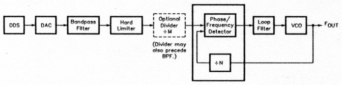
Figure 14-Block diagram of a DDS-driven PLL. This approach simultaneously achieves fine steps and fast settling time by using a direct digital synthesizer as a variable reference for a conventional PLL.
Figure 14 block diagrams such a system: a PLL frequency synthesizer with a reference frequency generated by a DDS. The advantages of this approach are:
- Broad output span
- Extremely fine frequency resolution with constant steps
- Fast switching time
- Fast settling time
- Low phase noise
- Low spurious noise (the design uses no mixers)
- Relatively simple circuitry
A Qualcomm application note(11) I provides a detailed analysis of this type of synthesizer. Using this approach, I and others have constructed a microprocessor-controlled frequency synthesizer that covers 75 to 105 MHz based on 32-bit resolution. Its output steps are essentially 0.07 Hz in size. A microprocessor drives the DDS and the PLL.
The system uses a Harris HSP45IO2 DDS and a Phillips TDA8702 digital-toanalog converter to generate a variable reference. Its ' output, centered around 10.7 MHz, is fed to a Motorola MC145170 single-loop PLL after being cleaned up by an inexpensive 10.7-MHz crystal filter.
The system's lock-up time depends solely on the time constant of the loop filter associated with the Motorola chip, and this approximation synthesizer gives a maximum error of 0.1 Hz relative to the output. The reference frequency chosen is 100 kHz, and the loop bandwidth is adjustable from 100 Hz to 1 kHz by selecting the filter components.
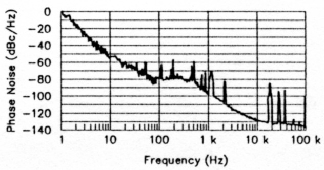
Figure 15-Measured phase noise for a practical system based on the DDSdriven-PLL technique of Figure 14. The test equipment used for this measurement and that of Figure 18 was a Hewlett-Packard HP3048A.
Figure 15 shows the SSB phase noise of the total system, which also uses a novel VCO (Figure 16). Figure 17 shows the predicted phase noise of this oscillator alone. Figure 18 shows the measured phase noise of the Kenwood TS-50's multi-loop synthesizer, a sound design, as a comparison. Comparing Figures 15 and 18 reveals the surprising fact that the simpler, wide-range single-VCO system is less phase-noisy than the TS-50. This is surprising because synthesized MF/HF equipment has long used multiple VCOs to cover a 30-MHz span solely because this approach allows VCO optimization for minimum phase noise. Achieving the same noise performance with a single VCO such as that shown in Figure 16 should allow us to reduce equipment cost, complexity and size without compromising phase-noise performance.
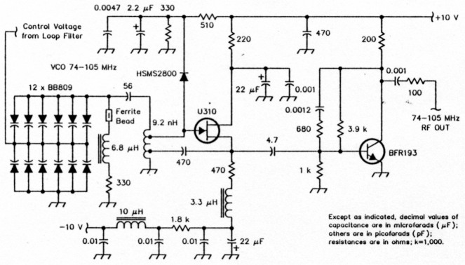
Figure 16-Circuit of the wideband VCO used in the system measured in Figure 15. Multiple tuning diodes are used to reduce the circuit's phase noise. The HSMS2800 diode at the U310's gate is reverse-biased and does not clip positive signal peaks like the gate-to-ground clamping diodes sometimes used in JFET oscillators by amateur builders. See text.
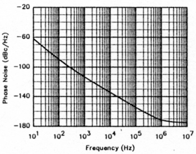
Figure 17-Predicted phase noise of the wide-band VCO alone.
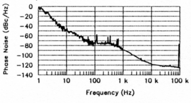
Figure 18-Measured phase noise of the TS-50 multi-loop synthesizer.
The gate diode in Figure 16 is reverse biased and does not clip the gate signal. In the past, some authors have recommended using clipping diodes to limit positive peaks at the gates of JFET oscillators.(12) if feedback is high in such an oscillator, the external diode can add significant noise to the oscillator output. Figure 19 shows that the noise increase due to a gate-clamping diode can be as high as 30 dB, but this effect is rarely mentioned in the literature. Note, however, that merely including a gate-clamping diode does not guarantee higher phase noise. Loose coupling between the JFET and tuned circuit may keep the gate voltage low enough so that the clamping diode does' not conduct. A nonconducting gate clamper adds no noise to the oscillator output.
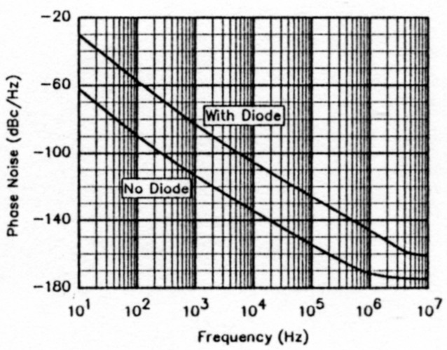
Figure 19-Predicted phase noise of the wide-band VCO with and without the gate-clamping diode long used by amateur builders in JFET VFOs. Depending on the feedback level, a gate-clamping diode can seriously degrade an oscillator's phase-noise performance. Gate bias achieved by means of a source resistor (see Note 12) is a better means of preventing gate-source conduction in a JFET oscillator.
Notes
- U. Rohde, "Recent Advances in Modern Shortwave Receiver Design," Part 1, QST, Nov 1992, pp 45-55, Fig 11.
- J. Porter, "AGC Loop Control Design Using System Theory," RF Design, Jun 1980, p 27.
- W. Sabin, "Use of Mixers in HF Upconversion Receivers/Exciters," Wescon/81, Professional Program Session Record 24, pp 24/1 to 24/4, Electronic Show and Convention, Sep 15-17, 1981.
- Even though two of the most popular Amateur Radio emissions (CW and SSB) are forms of amplitude modulation, AM as a concept and a technique receives relatively little attention from many radio amateurs today mainly because hamdom has largely abandoned full-carrier, double-sideband AM radiotelephony in favor of SSB radiotelephony. Meanwhile, "just across the hall" in commercial practice, high-quality AM transmission and reception are very much alive and up-to-date in the form of television and LF, MF and HF sound broadcasting. Amplifiers and amplifier devices designed for high-quality linear amplification of AM and wideband multiplexed signals, especially those intended for TV, satellite and cable-distribution service, are routinely threetone-tested to quantify their ability to simultaneously amplify multiple signals with minimal intermodulation and maximum linearity.-Ed.
- A complete survey of synthesizers for communications and testing equipment can be found in U. Rohde, Digital PLL Frequency Synthesizers-Theory and Design (Englewood Cliffs, NJ: Prentice-Hall Inc, 1983). This book is available from Compact Software, 201 McLean Blvd, Paterson, NJ 07504, tel 201-881-1200, fax 201-881-8361.
- "Hybrid PLUDDS Frequency Synthesis," Qualcomm Inc application note CL80-3459-1, Jun 1990.
- Experimenters have used the gate-clamping diode in JFET oscillators because (1) it disallows gate-junction conduction and greatly reduces the frequency drift that can indirectly result and (2) it is more experimenter-friendly than using a source bias resistor to accomplish the same thing because wide FET-toFET characteristics variation may make some copies of a given oscillator circuit fail to start if a particular source resistor value is specified. Two experiments at WJ1Z in converting existing gate-clamped JFET oscillators to source bias suggest, however, that a source resistance of 1 kΩ is a good initial value. (Hint: Good parts generally give better results, so also consider using a narrower-tolerance FET than the ubiquitous and mediocre MPF102 or 2N3819-a 2N4416, J310 or U310, for example.) The WJ1Z oscillators converted in this way (1) exhibited higher output than they did when gate-clamped and (2) were just as frequency stable with source bias as they were when gate-clamped.-Ed.
KA2WEU, Dr. Ulrich L. Rohde.