Design and construction of transistor power converters
It's economical to build your own transistor mobile power supply, but you have to know how to arrive at a satisfactory design. This article outlines the procedure. It also describes a high-power supply that you can duplicate without any paper work at all.
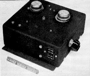
This mobile power supply is only six inches square, but delivers 120 watt of d.c. at 550 volt. The circuit is given in Fig. 6.
There has been a growing interest in transistorized power converters for mobile operation, because they are more efficient, more reliable, and can have less noise and ripple than either a vibrator type or a dynamotor. Over the past two years many articles on transistorized power converters with emphasis on the theory of operation(1) have been published. This paper is primarily intended to facilitate both calculations and construction. The following is a collection of design approximations and formulas suitable for an initial design. The major problems considered are core selection, transformer design and winding, feedback and bias design, and heat dissipation.
Core selection
The first problem to consider in designing a power converter is the selection of a transformer core. The selection of the core is controlled by several related variables, namely: saturation flux density, core area, available winding space and frequency. For a high-power converter - 100 watt - all of these must be considered but among them, available winding space is most important. Both the primary and secondary windings occupy appreciable volume; the primary has few turns of large wire and the secondary has many turns of small wire. The author has used successfully a toroidal core which has an inside diameter of 1.25 inches for a 100 watt converter. Any one of a variety of core materials which have a square hysteresis loop may be used. Materials such as Deltamax (Arnold Engineering Co., Marengo, Ill.) have been found satisfactory and economical.
Winding the transformer
There are three windings to be put on the core (Fig. 1). The primary should be first, the secondary may be next, and the feed-back winding last. There is a possibility that the feed-back turns might need modification after assembly, and winding the feed-back coil last enables such modifications to be made.
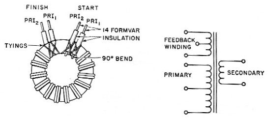
Fig. 1. Transformer winding details.
The number of primary and secondary turns can be calculated from the following formulas:
where:
Np = total turns in primary winding
A = cross-sectional area of core in square inches
Vs = d.c. input voltage
f = operating frequency in cycles per second
Bs = saturation flux of core in gausses
Ns = secondary turns
Eo = peak-to-peak output voltage required from transformer
A practical procedure for determining the number of primary turns is to work experimentally, using the formula as a check. First choose a wire size that will handle the current (see wire table in The Radio Amateur's Handbook). Then wind the maximum number of turns that will fill the inside circumference of the core following the procedure described below. Next, the formula may be used to find the expected frequency. This frequency should not be so high that the transistor switching times are an appreciable part of the cycle nor should it be too low since this will cause excessive copper losses. A frequency of about 1000 c.p.s. is optimum for most power transistors. If the calculated frequency is very much different from this the number of primary turns should be changed.
To protect the first layer of the winding, first wrap the core with Scotch electrical tape (acetate cloth) overlapping each turn about half the width of the tape on the inside surface of the core. Wind the primary first (Fig. 1). This winding must be bifilar to effectively eliminate spiking. To start, bend a 90-degree angle approximately 3 inches back from the ends of a pair of No. 14 Formvar wires. Insulate the two leads up to the first bend to protect against mechanical damage. Tie the two leads snugly to the core (Fig. 1). Proceed to wind the primary by keeping the wires tight, and square off the turns around the core. Finish the windings the same as they were started --i.e., the same insulation, tying, and so on. It is necessary to distribute the winding evenly around the inside circumference of the core for further suppression of spiking. Cover the entire primary winding with ½ inch wide crepe-paper tape.
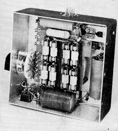
The transformer is not visible in this view, being mounted on the other side of the phenolic board that holds the silicon rectifiers and the bias resistors. The high-voltage bleeder resistors are at the lower left, between the filter capacitors and the output socket. The control relay is in the upper right corner.
To wind the secondary, a shuttle must be made. A Popsicle stick with a V cut in both ends makes an excellent shuttle. The shuttle will not hold enough wire to wind the complete secondary, so splices will have to be made. The supply can be made more versatile by making use of the splice points for output taps. For the first three or four times around the core, the secondary turns will lie between the primary wires on the outside circumference of the core. After that, the core should take a smooth doughnut shape. Finish by covering the windings with ½ inch crepe-paper tape.
Feedback and bias
Feedback and bias are very closely interrelated. Fig. 2 shows a simplified feed-back and bias network for the common-emitter configuration. Note that RI and R2 form a voltage divider that lowers base bias to enable oscillations to start. Note also that R1 is in series with the feedback windings. To compute the number of turns in the feed-back winding and the values of R1 and R2, proceed as follows: First choose the ratio of feed-back to primary-winding turns. A good approximation is 1/5 to 1/6. Then, for example, if NP = 36 turns,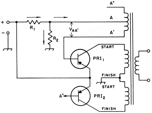
Fig. 2. Simplified feed-back and bias network for commas emitter configuration.
To continue the calculation, it is necessary to know the base voltage vs. collector current and base current vs. collector current characteristics of the transistor (Fig. 3), which may be obtained from the transistor manufacturer. From these curves we obtain the base voltage and current required for the desired power output. For a Delco 2N441, assuming a collector current of 12 amperes to get the required 100 watt output,
VB required = 1.1 V
IB required = 1.1 A.
Therefore
where ![]()
for proper cold starting. Therefore
A resistance of 100 ohms would be satisfactory, since the value of R2 is not highly critical.
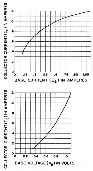
Fig. 3. These are typical power-transistor curves of the type used in calculating the bias-network constants in a transistor power supply.
Temperature and heat sinks
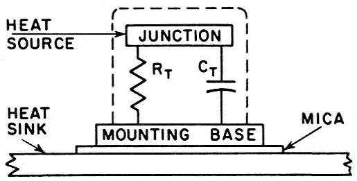
Fig. 4. Schematic representation of heat dissipation of transistor on heat sink.
It is necessary to provide a heat sink of the proper size to dissipate the heat developed at the collector junction. The chassis itself may be used for this purpose. The collector junction power, the maximum rated junction temperature, the thermal gradient, and the temperature drop from mounting base to heat sink (see Fig. 4) must be obtained from the manufacturer's data for calculating heat-sink area. The procedure is as follows:
1) Thermal Gradient (Delco 2N441)
Gradient from junction to mounting base (R5) = 1.2°C./watt
From base to mounting = 0.2°C./watt
Through mica washer = 0.5°C./watt
Therefore the total thermal gradient = 1.9°C./watt.
2) Collector Power
The measured power dissipated in one transistor while turned on was measured to be 8.5 watts (0.7 volt at 12 amp.). Because each transistor works half the time, this is also the average power for both transistors.
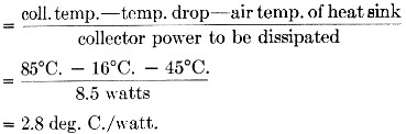
3) The temperature drop from collector junction to heat sink is therefore:
1.9°C./watt × 8.5 watt = 16°C.
4) If the maximum rated junction temperature is 85 °C., then the thermal resistance required of the heat-sink area is
The heat-sink area may now be determined from a curve of temperature vs. area (Fig. 5) supplied by the manufacturer. In the above case it is 60 square inches for two transistors. Thus there is no need to make the converter excessively large. In building most power converters the chassis, area required to mount the components (including the transformer, relay for switching, output voltage switch, output and input filters) is sufficiently large for adequate heat dissipation. For the example, the unit described below has a chassis area of 150 square inch.
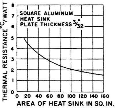
Fig. 5. Thermal resistance of 3/32 inch aluminum sheet.
A 120 Watt converter
Fig. 6 shows the circuit diagram of a converter designed to deliver 120 watt output, ICAS rating. Output power vs. efficiency and voltage are shown in Fig. 7. One method of checking the performance is to take a load curve. If all components - transistors, primary wire, secondary wire, and rectifiers - are within their maximum current ratings there should be no significant drop in efficiency at high power levels. If the efficiency curve begins to drop off at or near the power that the converter is expected to deliver, an optimum design has not been achieved and a dangerous heating condition may exist; the transistors are not driven into complete saturation and are absorbing an excessive portion of the input power. A decrease in the value of R1 usually will correct this condition.
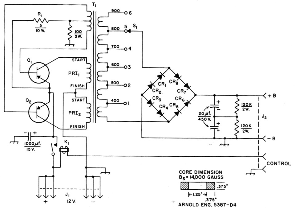
Fig. 6. Circuit of 120 watt power supply. Resistances are in ohms.
| CR1-CR8, inc. | Silicon rectifier, 500 mA, 400 volt inverse peak (Sarkes Tarzian M-500). |
| J1 | 6 contact male chassis-mounting connector (Jones). |
| J2 | Chassis-mounting connector, female, 4 or more contacts (Jones). |
| K1 | S.p.s.t. relay, 12 volt coil, 15-20 A contacts (Potter S, Brumfield MB series). |
| Q1,Q2 | P-n-p power transistors, 13 A, 40 volt breakdown (2N441). |
| R1 | 3 ohm, 10 watt. |
| S1 | Rotary, 1 section, 1 pole, 6 position. |
| T1 | Wound as described in text on core shown above. Primary, 36 turns No. 14 Formvar, center-tapped; secondary, 900 turns No. 26 Formvar, tapped at 400, 500, 600, 700 and 800 turns; feed-back winding, 15 turns No. 26 Formvar, center-tapped. |
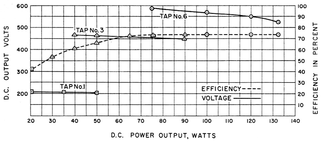
Fig. 7. Power output, output voltage, and supply efficiency of the transistor power-supply circuit shown in Fig. 6.
Because of the bifilar winding of the primary, no spike transients occurred in the design during the turn-off and turn-on of the transistors. This enabled good performance to be obtained with transistors having a 40 volt breakdown rating.
Construction of power converters would be an excellent club project. Items such as the acetate tape, crepe-paper tape and wire could be used more efficiently. Transistors, cores and diodes can be bought in volume much more cheaply, thus making the cost of such a project well below commercial prices.
Notes
- Chambers, "Transistorized power supply," QST, February, 1958.
Johnson, "High-power transistorized mobile power supply," QST, April, 1958.
Karl, "100 Watt transistor mobile power unit," QST, June, 1958.
J.G. Tetz, K2BQK.